

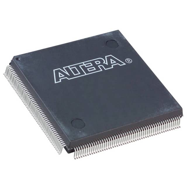
| Distributor | Stock | Pricing | MOQ | PKG | Lead Time | Date Code | On Order Quantity | On Order Delivery | |
|---|---|---|---|---|---|---|---|---|---|
|
3 pcs
|
3 pcs | On Request | 1 | On Request | On Request | On Request | On Request | On Request |
| Category | |
| Manufacturer Name | |
| Frequency | |
| Lead Spacing | |
| Mounting Type | |
| Number of Gates | |
| Number of I | |
| Number of I/O | |
| Number of LABs | |
| Number of Logic Elements | |
| Operating Temperature | |
| Supplier Device Package | |
| Supplier Package | |
| Total RAM Bits | |
| Voltage | |
| Voltage Supply |
The Intel EP1K100QC208-2N is a high-density programmable logic device from the ACEX 1K family. It offers 257,000 typical gates and 4,992 logic elements, making it suitable for complex system-on-a-programmable-chip (SOPC) integration.
This FPGA features 147 user I/O pins and 49,152 RAM bits, providing significant flexibility for various applications. It operates with a supply voltage range of 2.375V to 2.625V and has an operating temperature range of 0°C to 70°C (TA).
The device is packaged in a 208-PQFP (Plastic Quad Flat Pack) suitable for surface-mount applications. It supports bidirectional I/O performance up to 250 MHz and is compliant with the PCI Local Bus Specification Revision 2.2 for 3.3-V operation at 33 MHz or 66 MHz. It also includes JTAG boundary-scan test circuitry compliant with IEEE Std. 1149.1-1990.
Designed for high-volume applications, the EP1K100QC208-2N offers a cost-efficient programmable architecture. Development tools such as Quartus Software and Intel FPGA IP are available to support design efforts.
The EP1K100QC208-2N has 4,992 logic elements.
The EP1K100QC208-2N features 147 I/O pins.
The operating voltage range for the EP1K100QC208-2N is 2.375V to 2.625V.
The EP1K100QC208-2N is supplied in a 208-PQFP package.
The operating temperature range for the EP1K100QC208-2N is 0°C to 70°C (TA).
Yes, it is fully compliant with the Peripheral Component Interconnect Special Interest Group (PCI SIG) PCI Local Bus Specification, Revision 2.2 for 3.3-V operation at 33 MHz or 66 MHz.