

| Distributor | Stock | Pricing | MOQ | PKG | Lead Time | Date Code | On Order Quantity | On Order Delivery | |
|---|---|---|---|---|---|---|---|---|---|
|
16,436 pcs
|
16436 pcs | On Request | 1 | On Request | On Request | On Request | On Request | On Request | |
|
5,500 pcs
|
5500 pcs | On Request | 1 | On Request | On Request | On Request | On Request | On Request |
| Category | |
| Manufacturer Name | |
| Mounting Type | |
| Number of Gates | |
| Number of I | |
| Number of LABs | |
| Number of Logic Elements | |
| Operating Temperature | |
| Supplier Device Package | |
| Supplier Package | |
| Total RAM Bits | |
| Voltage |
The Intel EP1K100FC484-2N is a high-density programmable logic device (PLD) belonging to the ACEX 1K family. It provides system-on-a-programmable-chip (SOPC) integration capabilities within a single device.
Key features include 4992 logic elements (LEs) and 624 logic array blocks (LABs), supporting up to 257,000 typical gates. It offers 49,152 RAM bits for embedded memory functions and 333 user I/O pins for system interfacing. The device operates with a nominal internal supply voltage of 2.5V and is designed for a temperature range of 0°C to 70°C.
This FPGA is suitable for high-volume applications requiring cost-efficient programmable architecture. Its system-level features include MultiVolt I/O pins compatible with 2.5V, 3.3V, or 5.0V devices, and bidirectional I/O performance up to 250 MHz. The device is compliant with the PCI Local Bus Specification, Revision 2.2 for 3.3V operation at 33 MHz or 66 MHz.
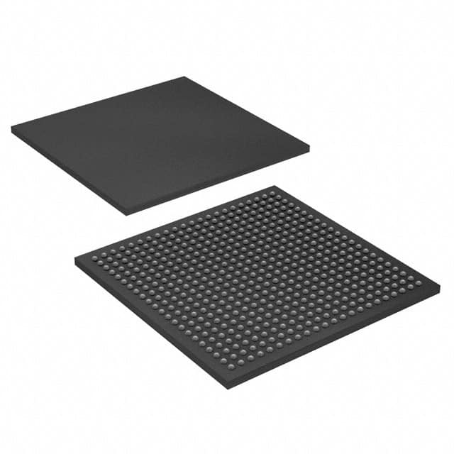
The EP1K100FC484-2N comes in a 484-FBGA (23x23) package and utilizes surface mount technology.
The typical gate count for the EP1K100FC484-2N FPGA is 257,000.
The EP1K100FC484-2N contains 4,992 logic elements.
This FPGA has a total of 49,152 RAM bits.
The EP1K100FC484-2N offers 333 user I/O pins.
The operating temperature range is 0°C to 70°C (TA).
The device operates with a voltage range of 2.375V to 2.625V, with a nominal internal supply voltage of 2.5V.
The EP1K100FC484-2N is supplied in a 484-FBGA (23x23) package, which is a surface mount type.