

| Distributor | Stock | Pricing | MOQ | PKG | Lead Time | Date Code | On Order Quantity | On Order Delivery | |
|---|---|---|---|---|---|---|---|---|---|
|
2 pcs
|
2 pcs | On Request | 1 | On Request | On Request | On Request | On Request | On Request |
| Category | |
| Manufacturer Name | |
| Lead Spacing | |
| Mounting Type | |
| Number of Gates | |
| Number of I | |
| Number of LABs | |
| Number of Logic Elements | |
| Operating Temperature | |
| Supplier Device Package | |
| Supplier Package | |
| Total RAM Bits | |
| Voltage |
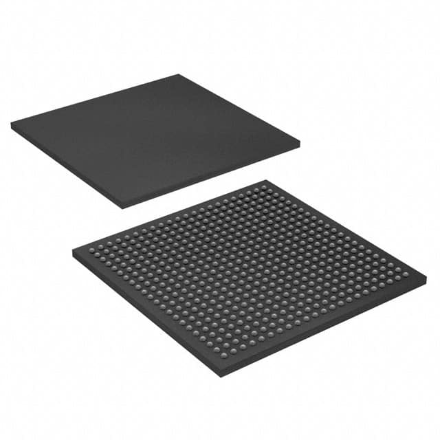
The Intel EP1K100FC484-1N is a field programmable gate array (FPGA) designed for embedded applications. It contains 4,992 logic elements, which are configurable logic blocks used for implementing digital circuits. The device also includes 49,152 bits of RAM, supporting complex data storage and processing tasks. With 333 input/output pins, it facilitates high connectivity for various system interfaces.
This FPGA operates at a voltage of 2.5V and is suitable for applications requiring high-density logic integration. It is packaged in a 484-BGA (ball grid array) form factor, specifically a 484-FBGA (23x23 mm), and is intended for surface mounting on printed circuit boards. The device complies with PCI Local Bus Specification Revision 2.2 and features IEEE Std. 1149.1-1990 JTAG boundary-scan test circuitry, enabling efficient testing and debugging.
Designed for embedded systems, this FPGA supports high-speed data processing and flexible logic configuration, making it suitable for telecommunications, industrial automation, and other high-performance digital applications.
The EP1K100FC484-1N contains 4,992 logic elements.
The package type is 484-BBGA.
The device has 333 I/O pins.
The operating voltage is 2.5V.