

| Distributor | Stock | Pricing | MOQ | PKG | Lead Time | Date Code | On Order Quantity | On Order Delivery | |
|---|---|---|---|---|---|---|---|---|---|
|
64,701 pcs
|
64701 pcs | On Request | 1 | On Request | On Request | 16+ | On Request | On Request |
| Category | |
| Manufacturer Name | |
| Configuration | |
| FET Feature | |
| Gate Charge (Qg) (Max) @ Vgs | |
| Halogen Free | |
| Junction Temperature | |
| Lead Style | |
| Mounting Type | |
| Operating Temperature | |
| Power | |
| Power Dissipation | |
| Storage Temperature | |
| Supplier Device Package | |
| Tape & Reel | |
| Technology |
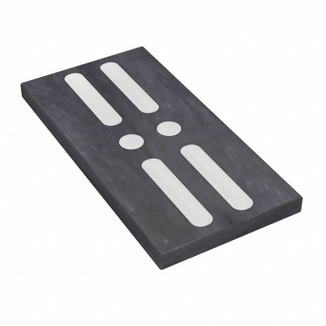
The EFC6611R-TF is a dual N-Channel MOSFET from On Semiconductor in a common-drain configuration. It is designed for 1-cell lithium-ion battery protection and power management applications. The device integrates two N-Channel MOSFETs with shared drain terminals, simplifying PCB layout for battery charging and discharging switches.
The MOSFET features a drain-to-source voltage (VSSS) rating of 12V and a gate-to-source voltage range of ±8V. It supports a continuous drain current of 27A and a pulsed current of 100A (100 µs pulse width, 1% duty cycle). The on-resistance is typically 2.3 mΩ at VGS=4.5V with a maximum of 3.2 mΩ, and 3.3 mΩ typical at VGS=3.1V (max 4.4 mΩ). Gate threshold voltage ranges from 0.5V to 1.3V at IS=1mA, making it suitable for logic-level drive. The device also features an ESD rating of 2 kV HBM and an ESD diode-protected gate.
The device is supplied in a surface-mount 6-CSP package (1.77x3.54 mm) with no leads, suitable for compact designs. Thermal resistance junction-to-ambient is 50°C/W when mounted on a ceramic substrate (5000 mm² x 0.8 mm). Maximum power dissipation is 2.5W, and the junction temperature can reach 150°C. The device is halogen-free, RoHS compliant, and Pb-Free.
Typical applications include 1-cell lithium-ion battery charging and discharging switches, power switching in portable devices, and load switching circuits. The common-drain configuration and low on-resistance make it efficient for battery protection circuits.
12 V.
6-SMD, No Lead (6-CSP 1.77x3.54 mm).
150°C.
Yes, the datasheet indicates Pb-Free, Halogen Free and RoHS compliance.
27 A.
0.5 V to 1.3 V at IS=1mA.
Yes, it is rated to 2 kV HBM.