

| Distributor | Stock | Pricing | MOQ | PKG | Lead Time | Date Code | On Order Quantity | On Order Delivery | |
|---|---|---|---|---|---|---|---|---|---|
|
1,738 pcs
|
1738 pcs | On Request | 1 | On Request | On Request | On Request | On Request | On Request | |
| On Request | On Request | 1 | On Request | On Request | On Request | On Request | On Request |
| Category | |
| Manufacturer Name | |
| Differential | |
| Frequency | |
| Input | |
| Lead Spacing | |
| Mounting Type | |
| Number of Circuits | |
| Operating Temperature | |
| Operating Voltage | |
| Output | |
| Power Dissipation | |
| Propagation Delay | |
| Ratio | |
| Supplier Device Package | |
| Type | |
| Voltage |
The DS90LV110TMTC from Texas Instruments is a high-speed differential 1 to 10 data/clock distributor utilizing LVDS technology. This device is designed for low power consumption and efficient signal distribution, making it suitable for replacing multi-drop bus applications requiring higher speeds and improved signal quality.
Key electrical specifications include a signaling rate of up to 800 Mbps and a maximum frequency of 400 MHz. It operates from a 3V to 3.6V supply voltage with a typical power dissipation of less than 413 mW. The device supports LVDS, LVPECL, and PECL input signals and provides LVDS output signals. Features like low jitter (145 ps typ), fast propagation delay (2.8 ns typ), and low output channel-to-channel skew (35 ps typ) ensure signal integrity.
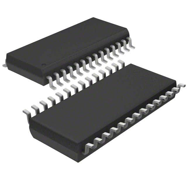
Packaged in a 28-lead TSSOP, the DS90LV110TMTC is designed for surface mount applications. It operates within an industrial temperature range of -40°C to 85°C. The fully differential data path from input to output minimizes noise generation and pulse width distortion, adhering to the ANSI/TIA/EIA-644 LVDS standard.
The operating temperature range is -40°C to 85°C.
The DS90LV110TMTC is available in a 28-TSSOP package.
The maximum signaling rate is 800 Mbps.
It supports LVDS, LVPECL, and PECL input signals and LVDS output signals.
The typical total power dissipation is less than 413 mW.