

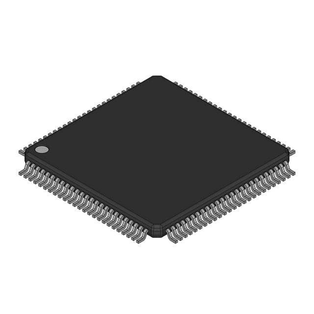
| Distributor | Stock | Pricing | MOQ | PKG | Lead Time | Date Code | On Order Quantity | On Order Delivery | |
|---|---|---|---|---|---|---|---|---|---|
|
1 pcs
|
1 pcs | On Request | 1 | On Request | On Request | On Request | On Request | On Request |
| Category | |
| Manufacturer Name | |
| Bandwidth | |
| Data Rate | |
| Function | |
| Input Type | |
| Lead Spacing | |
| Mounting Type | |
| Number of Inputs | |
| Number of Outputs | |
| Operating Temperature | |
| Output Type | |
| Storage Temperature | |
| Supplier Device Package | |
| Supplier Package | |
| Tape & Reel | |
| Voltage |
The DS90CR483VJD from Texas Instruments is a high-performance 48-bit LVDS Channel Link serializer/deserializer chipset. It is designed to convert 48 bits of CMOS/TTL data into eight LVDS data streams, transmitting data at rates up to 5.38 Gbps.
This device supports an input clock frequency range of 33 MHz to 112 MHz. Key features include LVDS SER/DES for reduced cable and connector size, user-selectable pre-emphasis to mitigate cable loading effects, and DC balancing for reduced ISI distortion. It also offers cable deskew capability of up to +/−1 LVDS data bit time.
The DS90CR483VJD operates with a supply voltage between 3V and 3.6V and has an operating temperature range of -10°C to 70°C (TA). It is packaged in a 100-TQFP (14x14) surface mount package, featuring a flow-through pinout for easy PCB design.
This chipset significantly reduces the number of conductors required compared to traditional parallel single-ended buses, offering system cost savings and reduced connector size. It is suitable for applications requiring high-speed data transmission over reduced cabling.
The operating voltage is between 3V and 3.6V.
The operating temperature range is -10°C to 70°C (TA).
It is available in a 100-TQFP (14x14) surface mount package.
The maximum data rate is 5.38 Gbps.
It supports input clock frequencies from 33 MHz to 112 MHz.
Yes, it features user-selectable pre-emphasis and DC balancing for data transmission.