

| Distributor | Stock | Pricing | MOQ | PKG | Lead Time | Date Code | On Order Quantity | On Order Delivery | |
|---|---|---|---|---|---|---|---|---|---|
|
3,287 pcs
|
3287 pcs | On Request | 1 | On Request | On Request | On Request | On Request | On Request |
| Category | |
| Manufacturer Name | |
| Bandwidth | |
| Mounting Type | |
| Operating Temperature | |
| Supplier Device Package | |
| Supplier Package | |
| Voltage |
The DS90CR287SLC/NOPB from Texas Instruments is a specialized interface IC functioning as a 28-bit Channel Link Transmitter. It is designed to convert 28 bits of LVCMOS/LVTTL data into four LVDS data streams, transmitting a phase-locked clock in parallel over a fifth LVDS link. This device operates at a supply voltage of 3.3V and supports shift clock frequencies ranging from 20 to 85 MHz.
With a maximum throughput of up to 2.38 Gbps and a bandwidth of 297.5 Mbytes/sec, the DS90CR287SLC/NOPB is engineered to address EMI and cable size challenges associated with high-speed TTL interfaces. It features a typical common-mode range of ±1V and a typical LVDS swing of 345 mV, contributing to low EMI.
The transmitter supports a 50% duty cycle on the receiver output clock and has set & hold times of 2.5 / 0 ns on TxINPUTs. It is compatible with the TIA/EIA-644 LVDS standard. The device operates within an ambient temperature range of -10 to 70 °C.
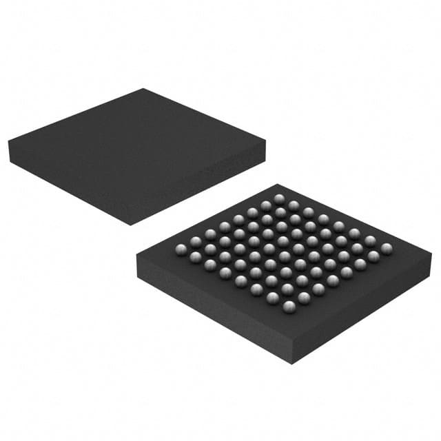
Available in a 64-NFBGA (8x8) package, the DS90CR287SLC/NOPB is designed for surface mount applications. Its architecture makes it suitable for applications requiring efficient and reliable high-speed data transmission over reduced cabling.
| Qty | Low | High |
|---|---|---|
| 1+ | $7.70 | $7.70 |
Estimated market price range - modelled values for guidance only, not live distributor offers.
The operating voltage is 3V to 3.6V.
The device is available in a 64-NFBGA (8x8) package and a 64-LFBGA package.
The operating temperature range is -10 to 70 °C.
The maximum data throughput is up to 2.38 Gbps.
It supports shift clock frequencies from 20 to 85 MHz.