

| Distributor | Stock | Pricing | MOQ | PKG | Lead Time | Date Code | On Order Quantity | On Order Delivery | |
|---|---|---|---|---|---|---|---|---|---|
|
120 pcs
|
120 pcs | On Request | 1 | On Request | On Request | 04+ | On Request | On Request |
| Category | |
| Manufacturer Name | |
| Bandwidth | |
| Operating Temperature | |
| SVHC Present | |
| Voltage |
The DS90CF388VJD from Texas Instruments is a Dual Pixel LVDS Display Interface (LDI) Receiver designed for SVGA/QXGA resolutions. It operates with a supply voltage of +3.3V and supports clock frequencies ranging from 40 to 112MHz, with a maximum bandwidth of 5.38Gbps.
This receiver is built to drive long, low-cost cables and features pre-emphasis to reduce cable loading effects. It offers a skew tolerance of 300ps for intra-pair skew and +/-1 LVDS data bit time for pair-to-pair skew at the receiver inputs. The dual pixel architecture facilitates interface to GUI and timing controllers, with optional single pixel transmitter inputs.
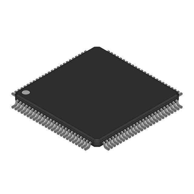
Designed for reliability, the DS90CF388VJD operates within an ambient temperature range of -10 to 70°C. It is housed in a 100-pin QFP (NEZ) package with dimensions of 256 mm² (16 mm × 16 mm). The device complies with the OpenLDI Specification for Digital Display Interfaces and is compatible with ANSI/TIA/EIA-644-1995 LVDS Standard.
| Qty | Low | High |
|---|---|---|
| 1+ | $4.78 | $4.78 |
Estimated market price range - modelled values for guidance only, not live distributor offers.
The operating temperature range is -10 to 70 °C.
The clock support for the DS90CF388VJD is 40 to 112 MHz.
The bandwidth is up to 5.38 Gbps.
The intra-pair skew tolerance is 300 ps.
The LVDS data bit time deskew is +/-1 LVDS Data Bit Time (up to 80 MHz Clock Rate).
The operating voltage is +3.3V.
The DS90CF388VJD is in a 100-pin QFP (NEZ) package.