

| Distributor | Stock | Pricing | MOQ | PKG | Lead Time | Date Code | On Order Quantity | On Order Delivery | |
|---|---|---|---|---|---|---|---|---|---|
|
2,004 pcs
|
2004 pcs | On Request | 1 | On Request | On Request | 24+ | On Request | On Request |
| Category | |
| Manufacturer Name | |
| Differential | |
| Frequency | |
| Input | |
| Input Voltage | |
| Lead Spacing | |
| Main Purpose | |
| Mounting Type | |
| Number of Circuits | |
| Operating Temperature | |
| Output | |
| Output Voltage | |
| PLL | |
| Ratio | |
| Supplier Device Package | |
| Supply Voltage | |
| Tape & Reel | |
| Termination | |
| Voltage |
The Analog Devices DS26502LN+ is a versatile building-integrated timing-supply (BITS) clock-recovery element that also functions as a basic T1/E1 transceiver. It is designed to recover clocks from various synchronization interfaces including T1, E1, 64kHz composite clock (64KCC), and 6312kHz synchronization timing. The device supports T1 and E1 modes, with the capability to recover and source Synchronization Status Message (SSM).
Key features include compliance with G.703 standards for synchronization interfaces, support for T1/J1 (1.544MHz) and E1 (2.048MHz), and CMI-coded interfaces. It offers a T1/E1 jitter attenuator with bypass mode and fully independent transmit and receive functionality. The DS26502LN+ includes internal software-selectable termination for various impedance values and accepts multiple master clock frequencies. Control can be managed via parallel, serial (SPI), or hardware ports, and it provides essential indications like LOS, AIS, and LOF.
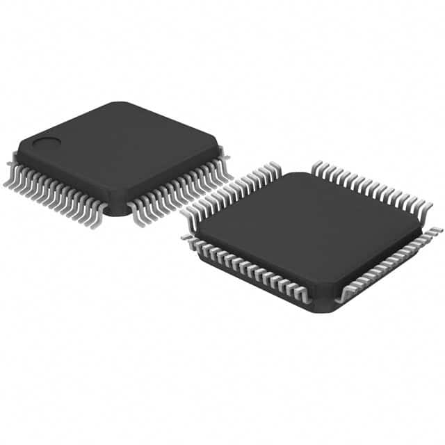
This component is housed in a 64-LQFP (10x10) Surface Mount package. It operates with a supply voltage of 3.135V to 3.465V and has 5V tolerant inputs and outputs. The operating temperature range is -40°C to 85°C, making it suitable for demanding environmental conditions. The device also features IEEE 1149.1 JTAG boundary scan for testing.
The operating temperature range is -40°C to 85°C.
The DS26502LN+ is available in a 64-LQFP (10x10) package.
The supply voltage is between 3.135V and 3.465V.
It supports G.703 2048kHz, G.703 64kHz, G.703 Appendix II 64kHz and 6312kHz Japanese, Standard T1/J1 (1.544MHz), and E1 (2.048MHz) interfaces.
Yes, it features a T1/E1 jitter attenuator with a bypass mode.
It can be controlled through an 8-bit parallel port (Intel or Motorola), a serial (SPI) port, or a hardware control mode.