


| Distributor | Stock | Pricing | MOQ | PKG | Lead Time | Date Code | On Order Quantity | On Order Delivery | |
|---|---|---|---|---|---|---|---|---|---|
|
1 pcs
|
1 pcs | On Request | 1 | On Request | On Request | On Request | On Request | On Request |
| Category | |
| Manufacturer Name | |
| Current | |
| Function | |
| Interface | |
| Lead Spacing | |
| Mounting Type | |
| Number of Circuits | |
| Operating Temperature | |
| Supplier Device Package | |
| Voltage |
The DS21552LN+ is a versatile single-chip transceiver designed for T1, J1, and E1 line interfaces. It integrates complete DS1/ISDN-PRI/J1 transceiver functionality, supporting both long and short haul LIU applications. The device features a crystal-less jitter attenuator and can generate DSX-1 and CSU line build-outs.
Key electrical specifications include a supply voltage range of 4.75V to 5.25V and a typical supply current of 75mA. It offers a fully independent transmit and receive functionality and includes an HDLC controller with 64-byte buffers. The interface supports E1, HDLC, J1, and T1 protocols.
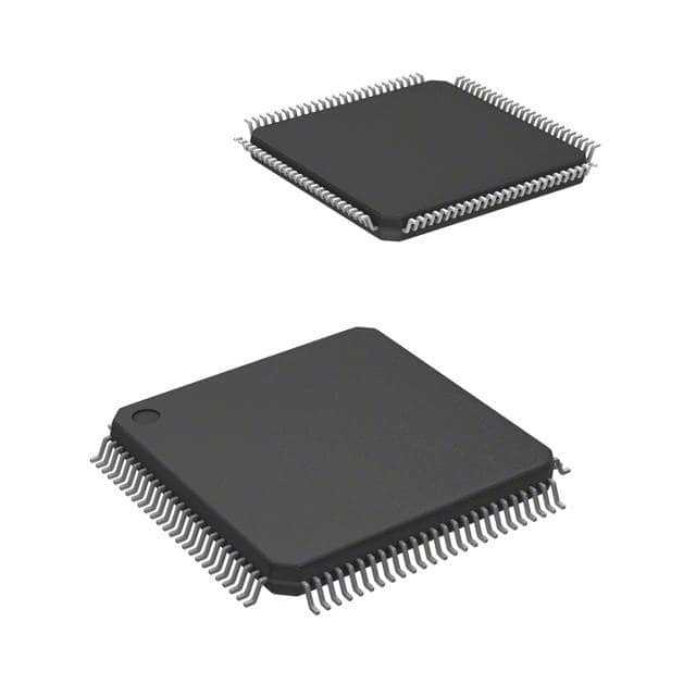
This transceiver is packaged in a 100-pin LQFP (14 mm x 14 mm) and is designed for surface mount applications. The operating temperature range is -40°C to 85°C, making it suitable for various environmental conditions. It also features IEEE 1149.1 JTAG-Boundary Scan for testing purposes.
The operating voltage for the DS21552LN+ is between 4.75V and 5.25V.
The DS21552LN+ operates in a temperature range of -40°C to 85°C.
The DS21552LN+ is supplied in a 100-LQFP package.
The DS21552LN+ supports E1, HDLC, J1, and T1 interface protocols.
Yes, the DS21552LN+ features IEEE 1149.1 JTAG-Boundary Scan.