

| Distributor | Stock | Pricing | MOQ | PKG | Lead Time | Date Code | On Order Quantity | On Order Delivery | |
|---|---|---|---|---|---|---|---|---|---|
|
46,020 pcs
|
46020 pcs | On Request | 1 | On Request | On Request | On Request | On Request | On Request |
| Category | |
| Manufacturer Name | |
| AEC Qualified | |
| Automotive Grade | |
| Configuration | |
| Current | |
| Drain to Source Voltage (Vdss) | |
| Gate Charge (Qg) (Max) @ Vgs | |
| Halogen Free | |
| Height (Max) | |
| Input Capacitance (Ciss) (Max) @ Vds | |
| Mounting Type | |
| Operating Temperature | |
| Power | |
| Rds On (Max) @ Id, Vgs | |
| Supplier Device Package | |
| Technology | |
| Termination Finish | |
| Vgs(th) (Max) @ Id | |
| Weight |
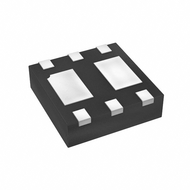
The DMP1046UFDB-7 is a dual P-Channel enhancement mode MOSFET manufactured by Diodes Incorporated. It is designed for low on-state resistance (RDS(on)) while maintaining superior switching performance, making it suitable for high-efficiency power management applications.
Key electrical characteristics include a drain-source voltage (Vdss) of 12V, maximum continuous drain current of 3.8A at Vgs=-4.5V, and maximum on-resistance of 61mΩ at Vgs=-4.5V. The device features low input capacitance (915pF at Vds=6V) and a gate charge of 17.9nC at Vgs=8V. The maximum gate threshold voltage is 1V at Id=250µA.
The MOSFET is housed in a compact 6-UDFN exposed pad package (U-DFN2020-6 Type B) with a low profile of 0.6mm maximum height. It supports surface mount assembly and is supplied in tape and reel packaging with 3000 units per reel. The device is rated for operation over a temperature range of -55°C to 150°C and has a power dissipation of 1.4W.
Environmental compliance includes RoHS3 compliance, lead-free construction, and halogen and antimony free (green device). Moisture sensitivity level is Level 1 per J-STD-020.
| Qty | Low | High |
|---|---|---|
| 1+ | $0.77 | $0.77 |
| 10+ | $0.48 | $0.48 |
| 25+ | $0.40 | $0.40 |
| 50+ | $0.35 | $0.35 |
| 100+ | $0.31 | $0.31 |
| 3,000+ | $0.18 | $0.18 |
| 9,000+ | $0.16 | $0.16 |
Estimated market price range - modelled values for guidance only, not live distributor offers.
The drain-source voltage (Vdss) is 12V.
The package is 6-UDFN Exposed Pad (U-DFN2020-6 Type B).
-55°C to 150°C.
Yes, it is RoHS3 compliant.
Maximum drain current is 3.8A at Vgs=-4.5V, 3.3A at -2.5V, and 2.8A at -1.8V.
Maximum Rds(on) is 61mΩ at Vgs=-4.5V, 81mΩ at -2.5V, and 115mΩ at -1.8V.
Maximum gate threshold voltage (Vgs(th)) is 1V at Id=250µA.