

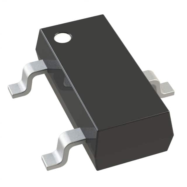
| Distributor | Stock | Pricing | MOQ | PKG | Lead Time | Date Code | On Order Quantity | On Order Delivery | |
|---|---|---|---|---|---|---|---|---|---|
|
2,450 pcs
|
2450 pcs | On Request | 1 | On Request | On Request | On Request | On Request | On Request |
| Category | |
| Manufacturer Name | |
| Automotive Grade | |
| Current | |
| Drain to Source Voltage (Vdss) | |
| Drive Voltage (Max Rds On, Min Rds On) | |
| FET Type | |
| Gate Charge (Qg) (Max) @ Vgs | |
| Halogen Free | |
| Input Capacitance (Ciss) (Max) @ Vds | |
| Mounting Type | |
| Operating Temperature | |
| Power Dissipation (Max) | |
| Rds On (Max) @ Id, Vgs | |
| Storage Temperature | |
| Supplier Device Package | |
| Tape & Reel | |
| Technology | |
| Termination Finish | |
| Vgs (Max) | |
| Vgs(th) (Max) @ Id | |
| Weight |
The DMN62D0UW-7 is an N-Channel enhancement mode MOSFET designed for high efficiency power management applications. It offers a maximum drain-source voltage of 60V and a continuous drain current of 340mA at 25°C ambient temperature. The device features a low on-resistance of 2Ω at VGS = 4.5V and 2.5Ω at VGS = 2.5V, enabling efficient switching with low conduction losses.
The MOSFET has a gate threshold voltage of 1V maximum at 250µA drain current, allowing operation with low gate drive voltages. It supports drive voltages of 1.8V and 4.5V for maximum and minimum on-resistance respectively. The device exhibits low input capacitance of 32pF at VDS = 30V and low gate charge of 0.5nC at VGS = 4.5V, contributing to fast switching speeds.
This component is housed in a compact SOT-323 surface mount package, suitable for space-constrained designs. It is rated for operation over a junction temperature range of -55°C to 150°C, with maximum power dissipation of 320mW at 25°C. The device includes an ESD protected gate for enhanced robustness.
The DMN62D0UW-7 is qualified to JEDEC standards for high reliability and is available in tape and reel packaging with 3,000 units per reel. It is suitable for motor control, power management functions, and backlighting applications.
| Qty | Low | High |
|---|---|---|
| 1+ | $0.28 | $0.28 |
| 10+ | $0.17 | $0.17 |
| 25+ | $0.14 | $0.14 |
| 50+ | $0.12 | $0.12 |
| 100+ | $0.11 | $0.11 |
| 3,000+ | $0.06 | $0.06 |
| 9,000+ | $0.05 | $0.05 |
Estimated market price range - modelled values for guidance only, not live distributor offers.
The maximum drain-source voltage (Vdss) is 60V.
The maximum continuous drain current is 340mA at TA = +25°C with Vgs = 4.5V.
The maximum on-resistance is 2Ω at Vgs = 4.5V and 2.5Ω at Vgs = 2.5V, both at Id = 100mA.
The operating junction temperature range is -55°C to 150°C.
Yes, the device is RoHS3 compliant and totally lead-free.
It is available in the SOT-323 surface mount package (SC-70, SOT-323).