

| Distributor | Stock | Pricing | MOQ | PKG | Lead Time | Date Code | On Order Quantity | On Order Delivery | |
|---|---|---|---|---|---|---|---|---|---|
|
10,000 pcs
|
10000 pcs | On Request | 1 | On Request | On Request | 18+ | On Request | On Request |
| Category | |
| Manufacturer Name | |
| Current | |
| Drain to Source Voltage (Vdss) | |
| Drive Voltage (Max Rds On, Min Rds On) | |
| FET Type | |
| Gate Charge (Qg) (Max) @ Vgs | |
| Halogen Free | |
| Input Capacitance (Ciss) (Max) @ Vds | |
| Mounting Type | |
| Operating Temperature | |
| Power Dissipation (Max) | |
| Rds On (Max) @ Id, Vgs | |
| Supplier Device Package | |
| Tape & Reel | |
| Technology | |
| Termination Finish | |
| UL Flammability Rating | |
| Vgs (Max) | |
| Vgs(th) (Max) @ Id | |
| Weight |
The DMN3730UFB4-7 is a 30V N-Channel enhancement mode MOSFET from Diodes Incorporated, designed for high efficiency power management applications. It features a maximum drain-source voltage of 30V and a continuous drain current of 750mA at 25°C ambient temperature. The device offers a low drain-source on-resistance of 460mΩ at VGS=4.5V and 560mΩ at VGS=2.5V, enabling efficient switching with minimal power loss.
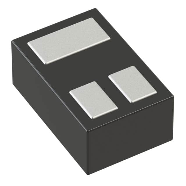
This MOSFET is housed in an ultra-compact X2-DFN1006-3 surface mount package with a 0.6mm² footprint, making it suitable for space-constrained portable applications. The package has an ultra-low profile of 0.4mm and weighs approximately 0.001 grams. It supports a gate-source voltage range of ±8V and has a maximum gate threshold voltage of 950mV at 250µA drain current, allowing direct drive from low-voltage sources.
The device is qualified to AEC-Q101 standards for high reliability automotive applications and features ESD protection of 2kV on the gate. It is totally lead-free, RoHS compliant, and halogen and antimony free, meeting modern environmental requirements. With an operating temperature range of -55°C to +150°C, it is suitable for demanding environments.
Typical applications include load switching, portable devices, and power management functions where space and efficiency are critical. The low gate charge of 1.6nC and input capacitance of 64.3pF contribute to fast switching performance, making it ideal for battery-powered and high-frequency circuits.
The maximum drain-source voltage (V(BR)DSS) is 30V.
The maximum continuous drain current is 750mA at TA=+25°C, and 0.91A at VGS=4.5V.
The maximum on-resistance is 460mΩ at VGS=4.5V and 560mΩ at VGS=2.5V.
It is available in the X2-DFN1006-3 surface mount package, which is a 3-XFDFN package with a 0.6mm² footprint.
The operating and storage temperature range is -55°C to +150°C.
Yes, it is fully RoHS compliant (RoHS3) and totally lead-free.
The maximum power dissipation is 470mW at TA=+25°C with minimum pad layout, and 0.69W with standard pad layout.