

| Distributor | Stock | Pricing | MOQ | PKG | Lead Time | Date Code | On Order Quantity | On Order Delivery | |
|---|---|---|---|---|---|---|---|---|---|
|
25,020 pcs
|
25020 pcs | On Request | 1 | On Request | On Request | On Request | On Request | On Request |
| Category | |
| Manufacturer Name | |
| Halogen Free | |
| Mounting Type | |
| Tape & Reel | |
| Weight |
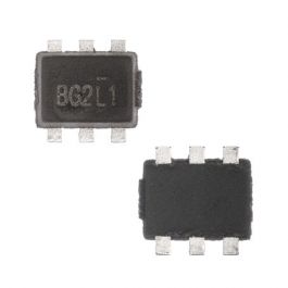
The Diodes Incorporated DMN32D0LV-7 is a dual N-channel enhancement mode field-effect transistor. It is engineered to minimize on-state resistance (RDS(ON)) while maintaining superior switching performance, making it suitable for high efficiency power management applications.
Key electrical characteristics include a Drain-Source Voltage (BVDSS) of 30V and a Gate-Source Voltage (VGSS) of ±10V. The on-resistance (RDS(ON)) is 1.2Ω at a gate-source voltage of 4.5V, with a continuous drain current (ID) of 0.68A under the same conditions. At a lower gate-source voltage of 2.5V, the RDS(ON) is 1.5Ω and the ID is 0.61A.
This MOSFET features a very low gate threshold voltage, low input capacitance, and fast switching speed, along with low input/output leakage. It is housed in an ultra-small SOT563 surface mount package, constructed from molded plastic with a UL Flammability Classification Rating of 94V-0. The terminals are finished with matte tin annealed over a copper leadframe, making them solderable per MIL-STD-202, Method 208.
| Qty | Low | High |
|---|---|---|
| 1+ | $0.99 | $0.99 |
Estimated market price range - modelled values for guidance only, not live distributor offers.
The Drain-Source Voltage (BVDSS) for the DMN32D0LV-7 is 30V.
The typical On-Resistance (RDS(ON)) at VGS = 4.5V is 1.2Ω.
The typical Drain Current (ID) at TA = +25°C and VGS = 4.5V is 0.68A.
The DMN32D0LV-7 is supplied in a SOT563 package.
Yes, the DMN32D0LV-7 is RoHS3 compliant.
The Moisture Sensitivity Level (MSL) for the DMN32D0LV-7 is Level 1.
Yes, the DMN32D0LV-7 is totally lead-free.