

| Distributor | Stock | Pricing | MOQ | PKG | Lead Time | Date Code | On Order Quantity | On Order Delivery | |
|---|---|---|---|---|---|---|---|---|---|
|
188 pcs
|
188 pcs | On Request | 1 | On Request | On Request | 17+ | On Request | On Request |
| Category | |
| Manufacturer Name | |
| Configuration | |
| Current | |
| Drain to Source Voltage (Vdss) | |
| Gate Charge (Qg) (Max) @ Vgs | |
| Halogen Free | |
| Input Capacitance (Ciss) (Max) @ Vds | |
| Mounting Type | |
| Operating Temperature | |
| Power | |
| Rds On (Max) @ Id, Vgs | |
| SVHC Present | |
| Supplier Device Package | |
| Tape & Reel | |
| Technology | |
| Termination Style | |
| Vgs(th) (Max) @ Id |
The DMN2300UFL4-7 is a 20V dual N-channel enhancement mode MOSFET from Diodes Incorporated, designed to minimize on-state resistance while maintaining superior switching performance. It features a maximum drain-source voltage of 20V and a continuous drain current of 2.11A at +25°C (Note 6). The on-resistance is specified at 195mΩ maximum at VGS = 4.5V with ID = 300mA, with additional ratings at lower gate voltages (260mΩ at 2.5V, 380mΩ at 1.8V, 520mΩ at 1.5V).
The gate threshold voltage is 950mV maximum at ID = 250µA, and the total gate charge is 3.2nC at VGS = 4.5V. Input capacitance is 128.6pF at VDS = 25V. The device is ESD protected and offers fast switching speed. Maximum power dissipation is 1.39W (Note 6) and 0.53W (Note 5), with an operating junction temperature range of -55°C to +150°C.
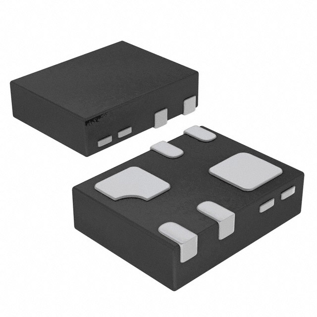
The MOSFET is housed in a surface-mount X2-DFN1310-6 package (case), which features a footprint of just 1.3mm² and an ultra-low profile of 0.4mm. The case material is molded plastic, green molding compound, with NiPdAu annealed over copper leadframe terminals. Thermal resistance from junction to ambient is 238°C/W (Note 5) and 90°C/W (Note 6). The part is supplied on 7-inch reels with 8mm tape, 3000 units per reel.
The maximum drain-source voltage (Vdss) is 20 V.
The continuous drain current is 2.11 A maximum at TA = +25°C (Note 6).
The maximum on-resistance is 195 mΩ at VGS = 4.5V and ID = 300mA. It is also specified as 260 mΩ at VGS = 2.5V, 380 mΩ at VGS = 1.8V, and 520 mΩ at VGS = 1.5V.
The device is housed in an X2-DFN1310-6 surface-mount package with exposed pad.
The operating junction temperature range is -55°C to +150°C.
The device is marked as RoHS3 Compliant (unverified) and is also described as Totally Lead-Free and fully RoHS compliant in the datasheet.