

| Distributor | Stock | Pricing | MOQ | PKG | Lead Time | Date Code | On Order Quantity | On Order Delivery | |
|---|---|---|---|---|---|---|---|---|---|
|
400 pcs
|
400 pcs | On Request | 1 | On Request | On Request | 24+ | On Request | On Request | |
|
340 pcs
|
340 pcs | On Request | 1 | On Request | On Request | 10+ | On Request | On Request |
| Category | |
| Manufacturer Name | |
| AEC Qualified | |
| Automotive Grade | |
| Current | |
| Drain to Source Voltage (Vdss) | |
| Drive Voltage (Max Rds On, Min Rds On) | |
| FET Type | |
| Gate Charge (Qg) (Max) @ Vgs | |
| Input Capacitance (Ciss) (Max) @ Vds | |
| Mounting Type | |
| Operating Temperature | |
| Power Dissipation (Max) | |
| Rds On (Max) @ Id, Vgs | |
| Supplier Device Package | |
| Tape & Reel | |
| Technology | |
| UL Flammability Rating | |
| Vgs (Max) | |
| Vgs(th) (Max) @ Id | |
| Weight |
The DMG6402LDM-7 is an N-Channel Enhancement Mode MOSFET from Diodes Incorporated. It is designed for general-purpose switching applications and features a maximum drain-source voltage of 30V and a continuous drain current of 5.3A at 25°C (4.2A at 70°C). The device offers a low on-resistance of 27mΩ maximum at VGS=10V and a typical RDS(on) of 22mΩ at VGS=4.5V. It also has low input capacitance (404pF typical) and fast switching characteristics with a typical turn-on delay of 3.41ns and rise time of 6.18ns.
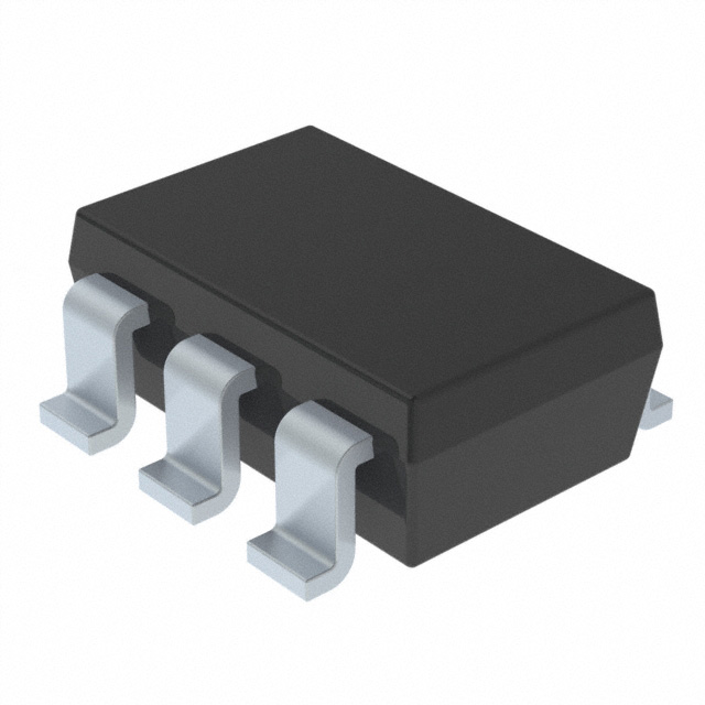
This MOSFET is housed in a compact SOT-26 (SOT-23-6) surface-mount package, weighing only 0.008 grams, making it suitable for space-constrained designs. The package has a UL flammability rating of 94V-0 and is MSL Level 1 per J-STD-020. The device is qualified to AEC-Q101 standards for high reliability, indicating suitability for automotive applications. It is RoHS compliant and lead-free by design.
Please note that this part is designated as 'NOT RECOMMENDED FOR NEW DESIGN' per the manufacturer's datasheet. The recommended replacement is the DMG6402LVT. For existing designs, the DMG6402LDM-7 remains available as a reliable component. Its thermal resistance from junction to ambient is 111°C/W when mounted on an FR-4 PCB with minimum recommended pad layout, and the power dissipation is 1.12W at 25°C.
| Qty | Low | High |
|---|---|---|
| 1+ | $0.67 | $0.67 |
| 10+ | $0.41 | $0.41 |
| 25+ | $0.34 | $0.34 |
| 50+ | $0.30 | $0.30 |
| 100+ | $0.26 | $0.26 |
| 3,000+ | $0.15 | $0.15 |
| 9,000+ | $0.13 | $0.13 |
Estimated market price range - modelled values for guidance only, not live distributor offers.
The maximum drain-source voltage (Vdss) is 30 V.
It is available in a SOT-23-6 package, also known as SOT-26.
The operating junction temperature range is -55°C to 150°C.
Yes, it is RoHS compliant and lead-free by design.
The continuous drain current is 5.3 A at 25°C and 4.2 A at 70°C.
The gate threshold voltage ranges from 1.0 V to 2.0 V, with a typical value of 1.5 V.
No, it is not recommended for new designs. The recommended replacement is the DMG6402LVT.