

| Distributor | Stock | Pricing | MOQ | PKG | Lead Time | Date Code | On Order Quantity | On Order Delivery | |
|---|---|---|---|---|---|---|---|---|---|
|
261 pcs
|
261 pcs | On Request | 1 | On Request | On Request | 11+ | On Request | On Request |
| Category | |
| Manufacturer Name | |
| AEC Qualified | |
| Automotive Grade | |
| Configuration | |
| Current | |
| Drain to Source Voltage (Vdss) | |
| FET Feature | |
| Gate Charge (Qg) (Max) @ Vgs | |
| Halogen Free | |
| Input Capacitance (Ciss) (Max) @ Vds | |
| Mounting Type | |
| Operating Temperature | |
| Power | |
| Rds On (Max) @ Id, Vgs | |
| SVHC Present | |
| Supplier Device Package | |
| Tape & Reel | |
| Technology | |
| Termination Finish | |
| Vgs(th) (Max) @ Id |
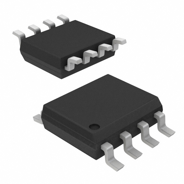
The DMC3021LSD-13 is a complementary pair enhancement mode MOSFET from Diodes Incorporated, combining an N-channel and a P-channel transistor in a single 8-SOIC surface mount package. The N-channel device (Q2) is rated for a drain-source voltage of 30V and a continuous drain current of 8.5A at 25°C, with a maximum on-resistance of 21mΩ at Vgs=10V. The P-channel device (Q1) is rated for -30V and -7A, with a maximum on-resistance of 53mΩ at Vgs=-4.5V. Both channels feature logic level gate drive capability, making them suitable for low-voltage control circuits.
The device is designed to minimize on-state resistance while maintaining superior switching performance, with a maximum gate charge of 16.1nC at Vgs=10V and input capacitance of 767pF at Vds=10V. The maximum gate threshold voltage is 2.1V at Id=250µA. Maximum power dissipation is 2.5W at 25°C ambient temperature, and the operating junction temperature range is -55°C to 150°C.
Typical applications include power management functions, analog switches, and load switches. The complementary pair configuration simplifies circuit design by providing both channel types in one package, reducing board space and component count. The device is housed in a standard 8-SOIC package (0.154" width, 3.90mm) with matte tin annealed over copper lead frame termination finish, and is available in tape and reel packaging with 2500 units per reel.
The DMC3021LSD-13 is totally lead-free and fully RoHS compliant, halogen and antimony free, and rated as a green device. It is qualified to JEDEC standards for high reliability.
| Qty | Low | High |
|---|---|---|
| 1+ | $1.19 | $1.19 |
| 10+ | $0.72 | $0.72 |
| 100+ | $0.51 | $0.51 |
| 500+ | $0.44 | $0.44 |
| 2,500+ | $0.44 | $0.44 |
Estimated market price range - modelled values for guidance only, not live distributor offers.
The drain-source voltage (Vdss) is 30V for the N-channel and -30V for the P-channel.
It comes in an 8-SOIC (0.154", 3.90mm Width) surface mount package, also referred to as SO-8.
The operating junction temperature range is -55°C to 150°C.
Yes, it is RoHS3 compliant per EU Directive 2011/65/EU and 2015/863/EU.
The N-channel can handle 8.5A continuous at 25°C, and the P-channel can handle -7A continuous at 25°C.
The N-channel has a maximum on-resistance of 21mΩ at Vgs=10V, Id=7A. The P-channel has a maximum on-resistance of 53mΩ at Vgs=-4.5V, Id=5.6A.
The maximum gate charge (Qg) is 16.1nC at Vgs=10V.