

| Distributor | Stock | Pricing | MOQ | PKG | Lead Time | Date Code | On Order Quantity | On Order Delivery | |
|---|---|---|---|---|---|---|---|---|---|
|
2,500 pcs
|
2500 pcs | On Request | 1 | On Request | On Request | On Request | On Request | On Request |
| Category | |
| Manufacturer Name | |
| Channel | |
| Channel Capacitance (CS(off), CD(off)) | |
| Charge Injection | |
| Crosstalk | |
| Current | |
| Lead Spacing | |
| Mounting Type | |
| Multiplexer | |
| Number of Circuits | |
| On | |
| Operating Temperature | |
| Power Consumption | |
| Supplier Device Package | |
| Switch Circuit | |
| Switch Time (Ton, Toff) (Max) | |
| Voltage |
The DG403CY is a dual, high-speed analog switch designed for efficient signal routing. It operates as a single-pole double-throw (SPDT) switch, with two independent circuits per device. Key electrical characteristics include a maximum on-resistance of 45 Ohms and fast switching times, with tON at 150ns and tOFF at 100ns.
This device supports a wide range of supply voltages, including single supply from +10V to +30V and bipolar supplies from ±4.5V to ±20V. It offers low charge injection of 10pC and low off-leakage current. The DG403CY is fabricated using a silicon-gate process and is designed for reliable performance over its operating temperature range of 0°C to 70°C.
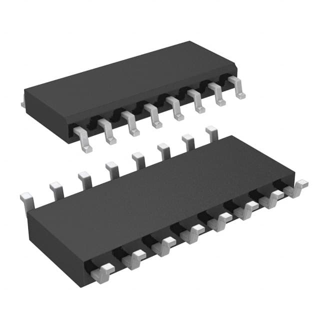
Packaged in a 16-SOIC surface-mount package, the DG403CY is suitable for integration into compact electronic systems. Its design makes it a plug-in upgrade for industry-standard parts, offering improved on-resistance matching and flatness between channels.
The maximum on-resistance of the DG403CY is 45 Ohms.
The maximum switching times for the DG403CY are 150ns for tON and 100ns for tOFF.
The DG403CY operates within a temperature range of 0°C to 70°C (TA).
The DG403CY is supplied in a 16-SOIC package.
The charge injection for the DG403CY is 10pC.