

| Distributor | Stock | Pricing | MOQ | PKG | Lead Time | Date Code | On Order Quantity | On Order Delivery | |
|---|---|---|---|---|---|---|---|---|---|
|
1,197 pcs
|
1197 pcs | On Request | 1 | On Request | On Request | On Request | On Request | On Request |
| Category | |
| Manufacturer Name | |
| AEC Qualified | |
| Applications | |
| Automotive Grade | |
| Core Processor | |
| Failure Rate | |
| Industrial Grade | |
| Interface | |
| Medical Grade | |
| Military Grade | |
| Mounting Type | |
| Number of I/O | |
| Operating Temperature | |
| Program Memory Type | |
| RAM Size | |
| Storage Temperature | |
| Supplier Device Package | |
| Tape & Reel | |
| Voltage Supply |
The Infineon CY8C20667S-24LQXI is a versatile Field Programmable Gate Array (FPGA) integrated with a microcontroller, designed for applications requiring flexible logic and control. It features an M8C core processor and 33 input/output pins, enabling complex interfacing and signal processing.
This device offers 32kB of FLASH program memory and 3K x 8 RAM, providing ample resources for custom configurations and data handling. The operating voltage range is from 1.71V to 5.5V, making it suitable for a variety of power-sensitive designs. The operating temperature range is -40°C to 85°C.
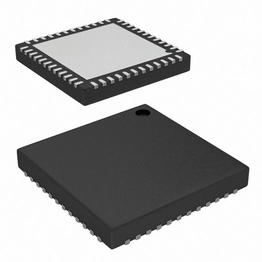
Packaged in a 48-UFQFN Exposed Pad, the CY8C20667S-24LQXI is designed for surface mounting. Its primary application is in capacitive sensing, leveraging its integrated capabilities for user interface and sensor management. The series is known as CapSense Controllers, indicating its suitability for touch-sensing solutions.
| Qty | Low | High |
|---|---|---|
| 1+ | $2.50 | $2.50 |
Estimated market price range - modelled values for guidance only, not live distributor offers.
The operating voltage range is 1.71V to 5.5V.
The CY8C20667S-24LQXI has 33 I/O pins.
The program memory type is FLASH with a size of 32kB.
The RAM size is 3K x 8.
The operating temperature range is -40°C to 85°C.
It is supplied in a 48-UFQFN Exposed Pad package.
The main applications include capacitive sensing.