

| Distributor | Stock | Pricing | MOQ | PKG | Lead Time | Date Code | On Order Quantity | On Order Delivery | |
|---|---|---|---|---|---|---|---|---|---|
|
7,000 pcs
|
7000 pcs | On Request | 1 | On Request | On Request | On Request | On Request | On Request |
| Category | |
| Manufacturer Name | |
| Clock Frequency | |
| Memory Format | |
| Memory Interface | |
| Memory Organization | |
| Memory Size | |
| Memory Type | |
| Mounting Type | |
| Operating Temperature | |
| Supplier Device Package | |
| Technology | |
| Termination | |
| Voltage |
The Infineon Technologies CY7C2265KV18-550BZXI is a high-performance 36-Mbit synchronous SRAM utilizing the QDR II+ architecture. This device offers a 550 MHz clock frequency, enabling high bandwidth operations. It features separate independent read and write data ports that support concurrent transactions, reducing the need for data bus turnaround.
The SRAM provides a 2.5 clock cycle read latency and a four-word burst architecture, which helps reduce the address bus frequency. It utilizes DDR interfaces on both read and write ports, allowing data transfer at 1100 MHz at the specified 550 MHz clock speed. The device operates with a core voltage of 1.8V ± 0.1V and supports I/O VDDQ from 1.4V to VDD, including both 1.5V and 1.8V I/O supplies.
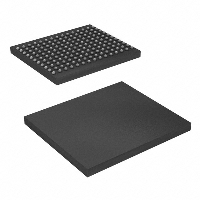
Designed for demanding applications, the CY7C2265KV18-550BZXI includes features such as on-die termination (ODT) for improved signal integrity and echo clocks (CQ and CQ) to simplify data capture in high-speed systems. It also features a data valid pin (QVLD) to indicate valid data on the output. The SRAM is housed in a 165-ball FBGA package measuring 13 x 15 x 1.4 mm, suitable for surface mount applications.
This SRAM is configured as 1M x 36 and is suitable for applications requiring fast, synchronous memory access. Its robust feature set and high clock speed make it a strong choice for complex digital systems.
| Qty | Low | High |
|---|---|---|
| 1+ | $1.28 | $1.28 |
Estimated market price range - modelled values for guidance only, not live distributor offers.
The clock frequency is 550 MHz.
The memory size is 36Mbit.
The operating voltage is 1.7V to 1.9V.
It is supplied in a 165-LBGA package.
The operating temperature range is -40°C to 85°C (TA).
The read latency is 2.5 clock cycles.