

| Distributor | Stock | Pricing | MOQ | PKG | Lead Time | Date Code | On Order Quantity | On Order Delivery | |
|---|---|---|---|---|---|---|---|---|---|
|
489 pcs
|
489 pcs | On Request | 1 | On Request | On Request | On Request | On Request | On Request |
| Category | |
| Manufacturer Name | |
| Frequency | |
| Logic Type | |
| Mounting Type | |
| Operating Temperature | |
| Operating Voltage | |
| Storage Temperature | |
| Tape & Reel |
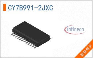
The Infineon CY7B991-2JXC is a clock buffer IC designed for signal distribution applications. It provides 8 inputs and 8 outputs, capable of operating at frequencies up to 80 MHz. This device utilizes TTL logic levels and requires an operating voltage range of 4.5V to 5.5V.
The CY7B991-2JXC is housed in a 32-PLCC package, suitable for surface mount applications. Its operating temperature range is from 0°C to 70°C. This component is part of Infineon's clock buffer offerings, designed to meet the demands of various electronic systems requiring precise clock signal management.
| Qty | Low | High |
|---|---|---|
| 1+ | $12.91 | $12.91 |
Estimated market price range - modelled values for guidance only, not live distributor offers.
The operating voltage for the CY7B991-2JXC is between 4.5V and 5.5V.
The CY7B991-2JXC clock buffer operates at a maximum frequency of 80 MHz.
The CY7B991-2JXC uses TTL logic.
The CY7B991-2JXC is available in a 32-PLCC package.
The operating temperature range for the CY7B991-2JXC is 0°C to 70°C.