

| Distributor | Stock | Pricing | MOQ | PKG | Lead Time | Date Code | On Order Quantity | On Order Delivery | |
|---|---|---|---|---|---|---|---|---|---|
|
4,512 pcs
|
4512 pcs | On Request | 1 | On Request | On Request | On Request | On Request | On Request |
| Category | |
| Manufacturer Name | |
| Halogen Free | |
| Lead Style | |
| Military Grade | |
| Operating Temperature Range | |
| Package Quantity |
The CY54FCT841ATDMB from Texas Instruments is a 10-bit bus-interface D-type latch designed for buffering existing latches and providing additional data width for wider address/data paths or buses carrying parity. These devices are buffered 10-bit-wide versions of the FCT373 function.
Key features include compatibility with FCT, F, and AM29841 logic, edge-rate control for improved noise characteristics, and support for partial-power-down mode operation with Ioff circuitry. The latches offer matched rise and fall times and ESD protection exceeding JESD 22 standards.
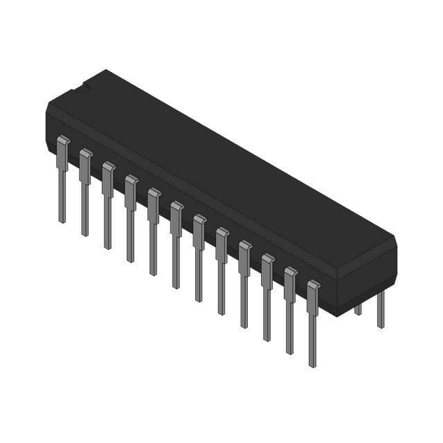
This component is fully compatible with TTL input and output logic levels, providing high-speed parallel latching with a buffered common latch-enable input and 3-state outputs. The CY54FCT841ATDMB is housed in a 24-pin CDIP (JT) package and operates within a temperature range of -55 to 125°C.
Applications for this device include systems requiring high-capacitance-load drive capability while maintaining low-capacitance bus loading. The Ioff circuitry is beneficial for partial-power-down applications, preventing damaging current backflow when the device is powered down.
| Qty | Low | High |
|---|---|---|
| 1+ | $28.99 | $28.99 |
Estimated market price range - modelled values for guidance only, not live distributor offers.
The operating temperature range is -55 to 125°C.
It is available in a 24-pin CDIP (JT) package.
The output sink current is 32mA for the CY54FCT841T.
The output source current is 12mA for the CY54FCT841T.
Yes, it supports partial-power-down mode operation.