

| Distributor | Stock | Pricing | MOQ | PKG | Lead Time | Date Code | On Order Quantity | On Order Delivery | |
|---|---|---|---|---|---|---|---|---|---|
|
3,303 pcs
|
3303 pcs | On Request | 1 | On Request | On Request | On Request | On Request | On Request |
| Category | |
| Manufacturer Name | |
| Frequency | |
| Input Type | |
| Mounting Type | |
| Number of Outputs | |
| Operating Temperature | |
| Operating Voltage | |
| Output Type |
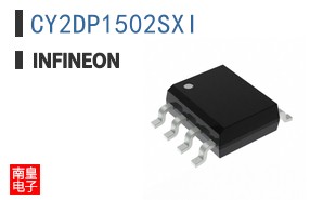
The Infineon CY2DP1502SXI is a high-performance clock buffer integrated circuit. It operates at a frequency of 1.5 GHz, making it suitable for demanding timing applications. The device supports multiple output types including CML, HCSL, LVDS, and LVPECL, with LVPECL being its primary output.
This clock buffer operates within a voltage range of 2.375V to 3.465V and functions across an industrial temperature range of -40°C to 85°C. It is housed in a standard 8-SOIC surface-mount package, measuring 0.154 inches (3.90mm) wide.
The CY2DP1502SXI is designed for applications requiring precise clock signal distribution and buffering. Its specifications make it a versatile component for various electronic systems where reliable clocking is critical.
| Qty | Low | High |
|---|---|---|
| 1+ | $12.91 | $12.91 |
Estimated market price range - modelled values for guidance only, not live distributor offers.
The operating voltage for the CY2DP1502SXI is between 2.375V and 3.465V.
The operating temperature range for the CY2DP1502SXI is -40°C to 85°C.
The CY2DP1502SXI is available in an 8-SOIC surface mount package.
The CY2DP1502SXI clock buffer operates at a frequency of 1.5 GHz.
The CY2DP1502SXI supports CML, HCSL, LVDS, and LVPECL output types, with LVPECL being the primary output.