

| Distributor | Stock | Pricing | MOQ | PKG | Lead Time | Date Code | On Order Quantity | On Order Delivery | |
|---|---|---|---|---|---|---|---|---|---|
|
5,570 pcs
|
5570 pcs | On Request | 1 | On Request | On Request | On Request | On Request | On Request |
| Category | |
| Manufacturer Name | |
| Frequency | |
| Input Type | |
| Mounting Type | |
| Operating Temperature | |
| Operating Voltage | |
| Output Type | |
| Storage Temperature | |
| Tape & Reel |
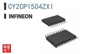
The Infineon CY2CP1504ZXI is a clock buffer designed for signal distribution applications. It offers a 2:4 input to output ratio, enabling it to buffer a single clock input to multiple outputs. The device operates with a maximum frequency of 250 MHz, making it suitable for various timing-critical systems.
This clock buffer utilizes LVCMOS signaling for its input and LVPECL for its output, providing compatibility with different logic families. The operating voltage range is from 2.375V to 3.465V. The CY2CP1504ZXI is housed in a 20-TSSOP surface mount package, requiring standard pick-and-place assembly processes.
Its operating temperature range is -40°C to 85°C, ensuring reliable performance in diverse environmental conditions. The component is designed for applications requiring precise clock signal management and distribution.
| Qty | Low | High |
|---|---|---|
| 1+ | $0.99 | $0.99 |
Estimated market price range - modelled values for guidance only, not live distributor offers.
The operating voltage range is 2.375V to 3.465V.
The maximum frequency is 250 MHz.
It supports LVCMOS input and LVPECL output.
The operating temperature range is -40°C to 85°C.
It is supplied in a 20-TSSOP package.