

| Distributor | Stock | Pricing | MOQ | PKG | Lead Time | Date Code | On Order Quantity | On Order Delivery | |
|---|---|---|---|---|---|---|---|---|---|
|
4,520 pcs
|
4520 pcs | On Request | 1 | On Request | On Request | On Request | On Request | On Request |
| Category | |
| Manufacturer Name | |
| AEC Qualified | |
| Automotive Grade | |
| Differential | |
| Frequency | |
| Industrial Grade | |
| Input | |
| Lead Spacing | |
| Medical Grade | |
| Military Grade | |
| Mounting Type | |
| Number of Circuits | |
| Operating Temperature | |
| Output | |
| Ratio | |
| Supplier Device Package | |
| Supplier Package | |
| Tape & Reel | |
| Type | |
| Voltage |
The Infineon Technologies CY2CP1504ZXI is a clock buffer IC designed for efficient signal distribution in electronic systems. This device offers a 2:4 fanout ratio, meaning it can take one input clock signal and distribute it to four output signals.
Key electrical specifications include an operating frequency of up to 250 MHz, supporting high-speed applications. It accepts LVCMOS input signals and provides LVPECL outputs, ensuring compatibility with various system architectures. The operating voltage range is from 2.375V to 3.465V, suitable for many digital designs.
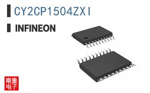
This clock buffer operates within a temperature range of -40°C to 85°C, making it robust for different environmental conditions. The component is supplied in a 20-TSSOP package, a common surface-mount form factor that facilitates integration onto printed circuit boards. Its mounting type is surface mount, requiring standard SMT assembly processes.
The CY2CP1504ZXI has a fanout ratio of 2:4.
The maximum operating frequency is 250 MHz.
It uses a 20-TSSOP surface mount package.
The operating voltage range is from 2.375V to 3.465V.
It supports LVCMOS input signals.
It produces LVPECL output signals.
The operating temperature range is from -40°C to 85°C.