

| Distributor | Stock | Pricing | MOQ | PKG | Lead Time | Date Code | On Order Quantity | On Order Delivery | |
|---|---|---|---|---|---|---|---|---|---|
|
30 pcs
|
30 pcs | On Request | 1 | On Request | On Request | On Request | On Request | On Request |
| Category | |
| Manufacturer Name | |
| AEC Qualified | |
| Automotive Grade | |
| Industrial Grade | |
| Input | |
| Medical Grade | |
| Military Grade | |
| Mounting Type | |
| Number of Circuits | |
| Operating Temperature | |
| Output | |
| PLL | |
| Storage Temperature | |
| Tape & Reel | |
| Voltage Supply |
The Infineon CY2309CZXC-1H is a high-performance clock buffer designed for various timing applications. It features a single input that drives nine LVCMOS outputs, providing a 1:9 ratio.
This device operates with a supply voltage range of 3V to 3.6V and can function in temperatures from 0°C to 70°C. The maximum operating frequency is 133.33MHz, making it suitable for demanding clock distribution needs. It includes a PLL with bypass functionality for flexible clock management.
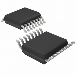
The CY2309CZXC-1H is available in a 16-pin TSSOP package, designed for surface mounting. Its input is compatible with LVCMOS and LVTTL logic levels, while its outputs are LVCMOS.
Key specifications include a 1:9 input to output ratio, a maximum frequency of 133.33MHz, and a 3V to 3.6V supply voltage. The operating temperature range is 0°C to 70°C. It is packaged in a 16-TSSOP tube.
| Qty | Low | High |
|---|---|---|
| 1+ | $12.91 | $12.91 |
Estimated market price range - modelled values for guidance only, not live distributor offers.
The maximum operating frequency is 133.33MHz.
The input to output ratio is 1:9.
The operating voltage range is 3V to 3.6V.
The operating temperature range is 0°C to 70°C.
It is supplied in a 16-TSSOP package.
Yes, it has a PLL with bypass functionality.