

| Distributor | Stock | Pricing | MOQ | PKG | Lead Time | Date Code | On Order Quantity | On Order Delivery | |
|---|---|---|---|---|---|---|---|---|---|
|
4 pcs
|
4 pcs | On Request | 1 | On Request | On Request | On Request | On Request | On Request |
| Category | |
| Manufacturer Name | |
| Differential | |
| Divider | |
| Frequency | |
| Input | |
| Input Type | |
| Mounting Type | |
| Number of Circuits | |
| Number of Outputs | |
| Operating Temperature | |
| Output | |
| PLL | |
| Ratio | |
| Supplier Device Package | |
| Supplier Package | |
| Type | |
| Voltage |
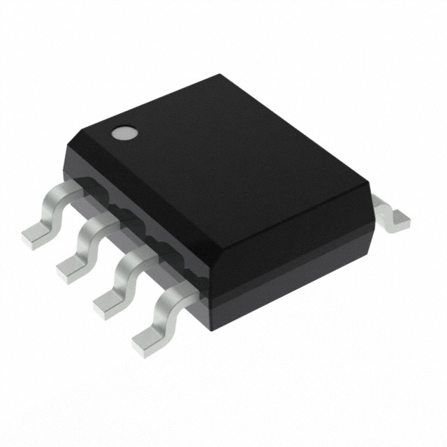
The Infineon Technologies CY2305CSXC-1T is a 3.3V Zero Delay Clock Buffer, part of the CYPRESS™ Buffers family. This device is designed to distribute high-speed clocks with zero input and output propagation delay. It accepts one reference input and drives five low-skew outputs, making it suitable for applications requiring precise clock distribution.
The CY2305CSXC-1T operates in the frequency range of 10 MHz to 133 MHz and utilizes an on-chip Phase-Locked Loop (PLL) to lock onto the input clock. It offers a typical cycle-to-cycle jitter of 50 ps at 15 pF and 66 MHz. The buffer operates at 3.0V to 3.6V and is available in a compact 8-pin SOIC package, suitable for surface mount applications.
This buffer is designed for commercial, industrial, and automotive flows. The PLL enters a power-down mode when there are no rising edges on the REF input, reducing current draw to less than 12.0 µA for commercial temperature devices. The device is also available in a test mode to bypass the PLL, allowing the input clock to be directly applied to the outputs for chip and system testing.
The CY2305CSXC-1T operates at 3 V to 3.6 V.
The operating temperature range is 0°C to 70°C.
The CY2305CSXC-1T is available in an 8-SOIC package.
The maximum operating frequency is 133.33 MHz.
Yes, the CY2305CSXC-1T has an on-chip Phase-Locked Loop (PLL).
The CY2305CSXC-1T provides five outputs.