

| Distributor | Stock | Pricing | MOQ | PKG | Lead Time | Date Code | On Order Quantity | On Order Delivery | |
|---|---|---|---|---|---|---|---|---|---|
|
83 pcs
|
83 pcs | On Request | 1 | On Request | On Request | On Request | On Request | On Request |
| Category | |
| Manufacturer Name | |
| Differential | |
| Divider | |
| Frequency | |
| Input | |
| Mounting Type | |
| Number of Circuits | |
| Operating Temperature | |
| Output | |
| PLL | |
| Ratio | |
| Supplier Device Package | |
| Supplier Package | |
| Type | |
| Voltage |
The CY2305CSXC-1H from Infineon Technologies is a 3.3V Zero Delay Clock Buffer, serving as a die replacement for older CY2305 and CY2309 parts. This component is designed to distribute high-speed clocks efficiently, featuring on-chip phase-locked loops (PLLs) that lock to an input clock signal.
Key electrical specifications include an operating frequency range from 10 MHz to 133.33 MHz, with zero input and output propagation delay. It provides five low-skew LVCMOS outputs from a single LVCMOS/LVTTL input. The device operates within a voltage range of 3V to 3.6V and has a typical cycle-to-cycle jitter of 50 ps at 15 pF and 66 MHz.
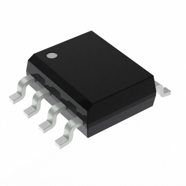
This buffer is available in an 8-pin SOIC package, suitable for surface mount applications. The operating temperature range is from 0°C to 70°C. The CY2305C and CY2309C PLLs enter a power-down mode when there are no rising edges on the REF input, reducing current draw to less than 12.0 µA for commercial temperature devices.
The operating frequency range is from 10 MHz to 133.33 MHz.
The CY2305CSXC-1H has zero input and output propagation delay.
The CY2305CSXC-1H provides five outputs from a single input.
The operating voltage is between 3V and 3.6V.
The operating temperature range is from 0°C to 70°C.
The CY2305CSXC-1H is available in an 8-pin SOIC package.