

| Distributor | Stock | Pricing | MOQ | PKG | Lead Time | Date Code | On Order Quantity | On Order Delivery | |
|---|---|---|---|---|---|---|---|---|---|
|
2,568 pcs
|
2568 pcs | On Request | 1 | On Request | On Request | On Request | On Request | On Request |
| Category | |
| Manufacturer Name | |
| Differential | |
| Frequency | |
| Input | |
| Input Capacitance | |
| Lead Spacing | |
| Load Capacitance | |
| Main Purpose | |
| Mounting Type | |
| Number of Circuits | |
| Operating Temperature | |
| Output | |
| PLL | |
| Ratio | |
| Supplier Device Package | |
| Supplier Package | |
| Voltage |
The CY2304NZZXC-1 from Infineon Technologies (formerly Cypress Semiconductor) is a versatile clock buffer designed to distribute high-speed clocks efficiently. It features a 1:4 output ratio, making it suitable for PCI-X and other general-purpose clock buffering needs.
This device operates from a 3.0V to 3.6V supply and can buffer frequencies from DC up to 140 MHz. Key electrical characteristics include low output-to-output skew, with a typical value of 60 ps and a maximum of less than 100 ps, ensuring precise clock signal timing. The input accepts LVCMOS and LVTTL signals, while the outputs are LVCMOS compatible.
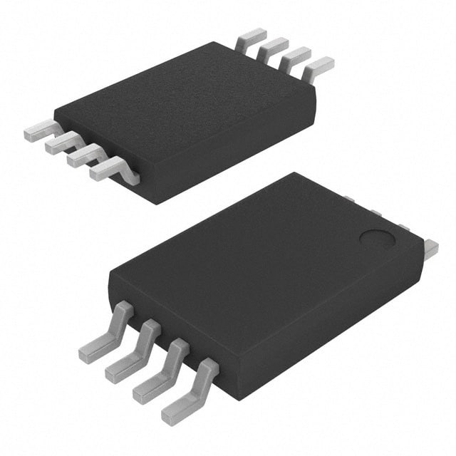
The CY2304NZZXC-1 is housed in a space-saving 8-pin TSSOP package, measuring 0.173 inches (4.40mm) in width. It is designed for surface mount applications. The operating temperature range is -40°C to 85°C, making it suitable for a variety of environmental conditions. The part also includes an output enable (OE) pin for control.
With its robust specifications and compact package, the CY2304NZZXC-1 is an excellent choice for applications requiring reliable clock signal distribution in systems where space and performance are critical.
| Qty | Low | High |
|---|---|---|
| 1+ | $13.57 | $13.57 |
Estimated market price range - modelled values for guidance only, not live distributor offers.
The CY2304NZZXC-1 can buffer frequencies from DC up to 140 MHz.
The device operates within a supply voltage range of 3.0V to 3.6V.
The CY2304NZZXC-1 is supplied in an 8-TSSOP package.
The operating ambient temperature range for this component is -40°C to 85°C.