

| Distributor | Stock | Pricing | MOQ | PKG | Lead Time | Date Code | On Order Quantity | On Order Delivery | |
|---|---|---|---|---|---|---|---|---|---|
|
146,998 pcs
|
146998 pcs | On Request | 1 | On Request | On Request | On Request | On Request | On Request | |
|
60,267 pcs
|
60267 pcs | On Request | 1 | On Request | On Request | On Request | On Request | On Request |
| Category | |
| Manufacturer Name | |
| Input Type | |
| Input Voltage | |
| Main Purpose | |
| Mounting Type | |
| Number of Circuits | |
| Operating Temperature | |
| Output Type |
The CY2304NZZI-1 from Infineon Technologies is an application-specific clock/timing integrated circuit designed for various applications. This IC operates at a maximum frequency of 140MHz, providing reliable clock signal generation.
It supports input voltages ranging from 3V to 3.6V, making it suitable for a wide array of electronic systems. The device is specified for operation across a temperature range of -40°C to 85°C, ensuring performance in diverse environmental conditions. The CY2304NZZI-1 features LVCMOS/LVTTL inputs and LVCMOS outputs, with a 1:4 input to output ratio.
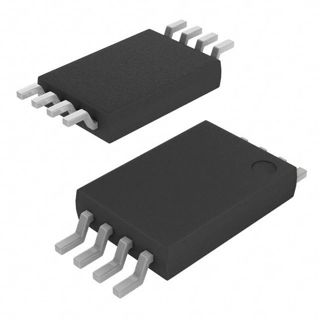
Packaged in an 8-TSSOP surface-mount configuration, this component is designed for efficient integration into printed circuit boards. Its robust design and specifications make it a valuable component for applications requiring precise clock timing.
| Qty | Low | High |
|---|---|---|
| 1+ | $12.91 | $12.91 |
Estimated market price range - modelled values for guidance only, not live distributor offers.
The maximum frequency for the CY2304NZZI-1 is 140MHz.
The CY2304NZZI-1 operates within a supply voltage range of 3V to 3.6V.
The operating temperature range for the CY2304NZZI-1 is -40°C to 85°C.
The CY2304NZZI-1 has LVCMOS and LVTTL inputs, and LVCMOS outputs.
The ratio of input to output for the CY2304NZZI-1 is 1:4.
The CY2304NZZI-1 is supplied in an 8-TSSOP package.