

| Distributor | Stock | Pricing | MOQ | PKG | Lead Time | Date Code | On Order Quantity | On Order Delivery | |
|---|---|---|---|---|---|---|---|---|---|
|
6,358 pcs
|
6358 pcs | On Request | 1 | On Request | On Request | On Request | On Request | On Request |
| Category | |
| Manufacturer Name | |
| Differential | |
| Divider | |
| Frequency | |
| Input | |
| Mounting Type | |
| Number of Circuits | |
| Operating Temperature | |
| Output | |
| PLL | |
| Propagation Delay | |
| Ratio | |
| Supplier Device Package | |
| Type | |
| Voltage | |
| Voltage Range |
The Infineon Technologies CY2302SXC-1 is a versatile frequency multiplier and zero delay buffer IC designed for clock generation applications. It features two outputs and supports a wide input frequency range from 5 MHz to 133 MHz, with configurable multiplication options.
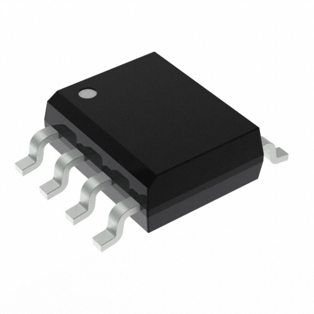
This device operates with a flexible voltage range of 3.3V ±5% or 5V ±10%, making it suitable for various system designs. Key electrical characteristics include typical jitter values of 90 ps for OUT2 and 200 ps for OUT1, with an output-to-output skew of 65 ps and a propagation delay of 90 ps. The CY2302SXC-1 is available in an 8-pin SOIC package and is designed for surface mount.
Configuration options allow for various frequency multiplications of the reference input, controlled by FS0 and FS1 pins. The part also includes an external feedback path for implementing the Zero Delay feature, offering maximum flexibility. Its input accepts LVCMOS and LVTTL signals, while the output is LVCMOS.
This component is suitable for applications requiring precise clock distribution and frequency synthesis. The 8-SOIC package and surface mount capability facilitate integration into compact electronic systems.
The CY2302SXC-1 operates at 3.3V or 5V.
The CY2302SXC-1 is available in an 8-SOIC package.
The operating temperature range is 0°C to 70°C.
The maximum output frequency is 133 MHz.
The typical jitter for OUT2 is 90 ps and for OUT1 is 200 ps.
The typical output-to-output skew is 65 ps.
The typical propagation delay is 90 ps.