

| Distributor | Stock | Pricing | MOQ | PKG | Lead Time | Date Code | On Order Quantity | On Order Delivery | |
|---|---|---|---|---|---|---|---|---|---|
|
1,520 pcs
|
1520 pcs | On Request | 1 | On Request | On Request | 1736+ | On Request | On Request |
| Category | |
| Manufacturer Name | |
| Avalanche Energy (Single Pulse) | |
| Configuration | |
| Continuous source current | |
| Drain To Source On Resistance (Maximum @ Vgs = 2.5 V) | |
| Drain To Source On Resistance (Maximum @ Vgs=4.5 V) | |
| Drain to Source Voltage (Vdss) | |
| Gate Charge (Qg) (Max) @ Vgs | |
| Gate Charge - Gate-to-Drain (Qgd) (Typical) | |
| Gate Charge - Gate-to-Source (Qgs) (Typical) | |
| Gate Threshold Voltage (Typical) | |
| Halogen Free | |
| Input Capacitance (Ciss) (Max) @ Vds | |
| Mounting Type | |
| Operating Temperature | |
| Package Type | |
| Power Dissipation | |
| Pulsed Source Current | |
| Standard Package Qty | |
| Supplier Device Package | |
| Tape & Reel | |
| Tape and Reel | |
| Technology | |
| Terminal Plating | |
| Vgs(th) (Max) @ Id |
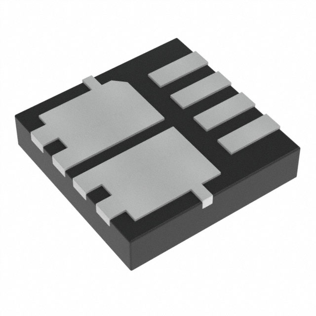
The CSD87313DMS is a 30V dual N-channel NexFET power MOSFET from Texas Instruments, configured as a common-drain pair. It is designed for USB Type-C and Power Delivery VBus protection, battery protection, and load-switch applications. The device is packaged in a compact 3.3mm x 3.3mm SON (8-WSON) plastic package with lead-free terminal plating.
Key electrical specifications include a maximum on-resistance of 5.5mΩ at VGS=4.5V and 9.6mΩ at VGS=2.5V. Total gate charge is 28nC typical at VGS=4.5V, with gate-to-drain charge of 6nC and gate-to-source charge of 6.3nC. Input capacitance is 4290pF maximum at VDS=15V. The device supports continuous source current of 17A and pulsed current up to 120A, with maximum power dissipation of 2.7W at TA=25°C when mounted on a 1-in² copper pad.
The common-drain configuration and low source-to-source on-resistance help minimize conduction losses in series-switch topologies. It is avalanche rated with single-pulse avalanche energy of 67mJ. The logic-level threshold voltage (typical 0.9V, maximum 1.25V) allows direct drive from 5V gate-drive circuits.
The CSD87313DMS operates over a junction temperature range of -55°C to 150°C and is surface-mount only. It is RoHS compliant and halogen free.
| Qty | Low | High |
|---|---|---|
| 1+ | $2.39 | $2.39 |
| 10+ | $1.52 | $1.52 |
| 100+ | $1.03 | $1.03 |
| 500+ | $0.83 | $0.83 |
| 1,000+ | $0.74 | $0.74 |
| 2,500+ | $0.66 | $0.66 |
Estimated market price range - modelled values for guidance only, not live distributor offers.
The drain-to-source voltage rating is 30V.
The CSD87313DMS comes in an 8-PowerWDFN package, also designated as 8-WSON (3.3mm x 3.3mm), for surface-mount assembly.
The operating temperature range is -55°C to 150°C (junction temperature).
Yes, the CSD87313DMS is RoHS3 compliant and halogen free, with lead-free terminal plating.
The maximum source-to-source on-resistance is 5.5mΩ at VGS=4.5V and 9.6mΩ at VGS=2.5V.
The continuous source current is 17A at TA=25°C, and pulsed current rating is 120A.
Total gate charge is 28nC typical at VGS=4.5V, with Qgd of 6nC and Qgs of 6.3nC.