

| Distributor | Stock | Pricing | MOQ | PKG | Lead Time | Date Code | On Order Quantity | On Order Delivery | |
|---|---|---|---|---|---|---|---|---|---|
|
116,100 pcs
|
116100 pcs | On Request | 1 | On Request | On Request | 1420+ | On Request | On Request |
| Category | |
| Manufacturer Name | |
| Configuration | |
| Current | |
| Drain to Source Voltage (Vdss) | |
| FET Feature | |
| Gate Charge (Qg) (Max) @ Vgs | |
| Halogen Free | |
| Input Capacitance (Ciss) (Max) @ Vds | |
| MEDIA | |
| Mounting Type | |
| Operating Temperature | |
| Power | |
| Rds On (Max) @ Id, Vgs | |
| Supplier Device Package | |
| Tape & Reel | |
| Technology | |
| Vgs(th) (Max) @ Id |
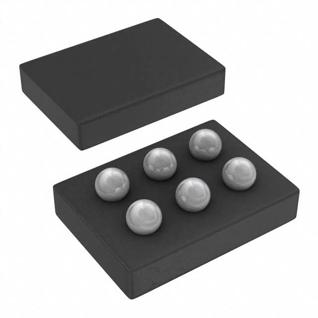
The CSD75301W1015 is a dual P-channel power MOSFET from Texas Instruments, part of the NexFET family. It features a common source configuration and is designed for space-constrained applications with a small 1.0mm × 1.5mm footprint and low profile of 0.62mm. The device offers ultra-low gate charge (Qg) of 1.5nC at 4.5V and low on-resistance, with RDS(on) as low as 80mΩ at VGS=-4.5V. Rated for a drain-source voltage of -20V and continuous drain current of -1.2A at TC=25°C, it operates over a junction temperature range of -55°C to 150°C. The MOSFET is available in a 6-DSBGA package and is supplied on tape and reel with 3000 units per reel. It is RoHS compliant and halogen free.
Typical applications include battery management, load switching, and battery protection circuits. The device also supports pulsed drain current up to 17.5A under specified conditions. With a gate threshold voltage typically -0.7V, it can be driven by low-voltage logic signals.
| Qty | Low | High |
|---|---|---|
| 647+ | $0.46 | $0.46 |
Estimated market price range - modelled values for guidance only, not live distributor offers.
-20V
6-UFBGA, DSBGA; supplier device package 6-DSBGA (1x1.5)
-55°C to 150°C (junction)
Yes, RoHS compliant and halogen free.
1.2A at TC=25°C
-0.7V typical, with range -0.4V to -1.0V
80mΩ typical, 100mΩ maximum