

| Distributor | Stock | Pricing | MOQ | PKG | Lead Time | Date Code | On Order Quantity | On Order Delivery | |
|---|---|---|---|---|---|---|---|---|---|
|
9,463 pcs
|
9463 pcs | On Request | 1 | On Request | On Request | 18 | On Request | On Request | |
|
1,574 pcs
|
1574 pcs | On Request | 1 | On Request | On Request | On Request | On Request | On Request |
| Category | |
| Manufacturer Name | |
| Current | |
| Drain to Source Voltage (Vdss) | |
| Drive Voltage (Max Rds On, Min Rds On) | |
| FET Type | |
| Gate Charge (Qg) (Max) @ Vgs | |
| Halogen Free | |
| Input Capacitance (Ciss) (Max) @ Vds | |
| Mounting Type | |
| Operating Temperature | |
| Power Dissipation (Max) | |
| Rds On (Max) @ Id, Vgs | |
| SVHC Present | |
| Supplier Device Package | |
| Tape & Reel | |
| Technology | |
| Vgs (Max) | |
| Vgs(th) (Max) @ Id |
The CSD25485F5 is a P-Channel MOSFET from Texas Instruments, designed for applications requiring efficient power switching in a compact form factor. It features a drain-source voltage (Vdss) of 20V and a continuous drain current of 3.2A at 25°C. The device offers low on-resistance, with a maximum of 35mΩ at 900mA and 8V gate drive, and 42mΩ at 4.5V gate drive, making it suitable for low-voltage, high-efficiency switching circuits.
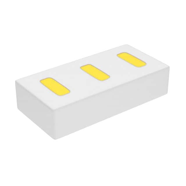
This MOSFET is logic-level compatible, with a maximum gate threshold voltage of 1.3V at 250µA, allowing direct drive from low-voltage logic circuits. It has a maximum gate-source voltage of -12V and a total gate charge of 3.5nC at 4.5V, contributing to fast switching and reduced power loss. The device is designed for surface-mount assembly in a 3-XFDFN package (3-PICOSTAR), which is ultra-small with a footprint of 1.53mm x 0.77mm and a low profile of 0.36mm, ideal for space-constrained handheld and mobile applications.
The CSD25485F5 operates over a temperature range of -55°C to 150°C, making it suitable for a wide range of environments. It is lead and halogen free, and is RoHS compliant. The device is designed for applications such as load switching, power management, and battery protection in portable electronics.
| Qty | Low | High |
|---|---|---|
| 1+ | $0.67 | $0.67 |
| 10+ | $0.41 | $0.41 |
| 100+ | $0.27 | $0.27 |
| 500+ | $0.20 | $0.20 |
| 1,000+ | $0.18 | $0.18 |
| 3,000+ | $0.15 | $0.15 |
| 6,000+ | $0.14 | $0.14 |
| 9,000+ | $0.12 | $0.12 |
| 24,000+ | $0.12 | $0.12 |
Estimated market price range - modelled values for guidance only, not live distributor offers.
The drain-source voltage (Vdss) is 20V.
The maximum continuous drain current is 3.2A at 25°C.
The maximum on-resistance is 35mΩ at 900mA and 8V gate drive, and 42mΩ at 4.5V gate drive.
The operating temperature range is -55°C to 150°C.
The package is 3-XFDFN, with a supplier device package of 3-PICOSTAR.
The device is marked as RoHS compliant and lead and halogen free.
The maximum gate threshold voltage is 1.3V at 250µA drain current.