

| Distributor | Stock | Pricing | MOQ | PKG | Lead Time | Date Code | On Order Quantity | On Order Delivery | |
|---|---|---|---|---|---|---|---|---|---|
|
35,107 pcs
|
35107 pcs | On Request | 1 | On Request | On Request | On Request | On Request | On Request | |
|
7,904 pcs
|
7904 pcs | On Request | 1 | On Request | On Request | 20+ | On Request | On Request | |
|
1,540 pcs
|
1540 pcs | On Request | 1 | On Request | On Request | On Request | On Request | On Request | |
|
500 pcs
|
500 pcs | On Request | 1 | On Request | On Request | 2026-02-25 06:16:38 | On Request | On Request | |
|
492 pcs
|
492 pcs | On Request | 1 | On Request | On Request | On Request | On Request | On Request | |
|
406 pcs
|
406 pcs | On Request | 1 | On Request | On Request | 20+18+ | On Request | On Request | |
|
10 pcs
|
10 pcs | On Request | 1 | On Request | On Request | 22+ | On Request | On Request |
| Category | |
| Manufacturer Name | |
| Configuration | |
| Current | |
| Drain to Source Voltage (Vdss) | |
| Drive Voltage (Max Rds On, Min Rds On) | |
| FET Type | |
| Gate Charge (Qg) (Max) @ Vgs | |
| Halogen Free | |
| Input Capacitance (Ciss) (Max) @ Vds | |
| Lead Style | |
| Mounting Type | |
| Operating Temperature | |
| Power Dissipation (Max) | |
| Rds On (Max) @ Id, Vgs | |
| SVHC Present | |
| Supplier Device Package | |
| Tape & Reel | |
| Technology | |
| Vgs (Max) | |
| Vgs(th) (Max) @ Id |
The CSD25402Q3A is a P-Channel NexFET power MOSFET from Texas Instruments, designed for power conversion and load management applications. It features a drain-source voltage rating of -20V and a gate-source voltage rating of -12V, with a single configuration. The device offers low on-resistance of 8.9mΩ (maximum) at VGS=4.5V and 15.9mΩ at VGS=2.5V, enabling efficient power handling.
This MOSFET is logic level compatible, with a typical gate threshold voltage of -0.9V, allowing direct drive from low-voltage logic circuits. It provides a continuous drain current of -72A (silicon limited at TC=25°C) and features ultra-low gate charge (QG typ 7.5nC, QGD typ 1.1nC, QGS typ 2.4nC), which reduces switching losses in high-frequency applications.
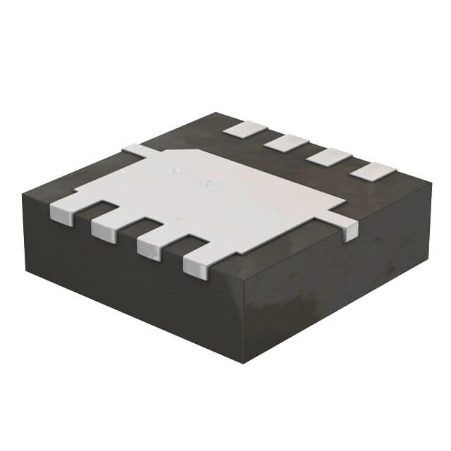
The device is housed in a SON 3.3mm x 3.3mm plastic package (VSONP DNH 8) with excellent thermal performance for its size, featuring low thermal resistance. It operates over a temperature range of -55°C to 150°C and is rated for catalog applications. The CSD25402Q3A is Pb and halogen free, and RoHS compliant, making it suitable for environmentally conscious designs.
Typical applications include power conversion circuits, load switches, and battery management systems where low conduction and switching losses are critical. The compact package and low thermal resistance support high-density PCB layouts.
| Qty | Low | High |
|---|---|---|
| 1+ | $1.32 | $1.32 |
| 10+ | $0.83 | $0.83 |
| 100+ | $0.55 | $0.55 |
| 500+ | $0.43 | $0.43 |
| 1,000+ | $0.39 | $0.39 |
| 2,500+ | $0.34 | $0.34 |
| 5,000+ | $0.31 | $0.31 |
Estimated market price range - modelled values for guidance only, not live distributor offers.
The drain-source voltage (VDS) rating is -20V.
The maximum on-resistance is 8.9mΩ at VGS=4.5V and 15.9mΩ at VGS=2.5V.
The operating temperature range is -55°C to 150°C.
Yes, the device is Pb and halogen free and RoHS compliant.
It is available in a SON 3.3mm x 3.3mm plastic package (VSONP DNH 8).