

| Distributor | Stock | Pricing | MOQ | PKG | Lead Time | Date Code | On Order Quantity | On Order Delivery | |
|---|---|---|---|---|---|---|---|---|---|
|
90,400 pcs
|
90400 pcs | On Request | 1 | On Request | On Request | On Request | On Request | On Request | |
|
8,942 pcs
|
8942 pcs | On Request | 1 | On Request | On Request | 15+ | On Request | On Request | |
|
5,695 pcs
|
5695 pcs | On Request | 1 | On Request | On Request | 11+ | On Request | On Request |
| Category | |
| Manufacturer Name | |
| Current | |
| Drain to Source Voltage (Vdss) | |
| Drive Voltage (Max Rds On, Min Rds On) | |
| FET Type | |
| Gate Charge (Qg) (Max) @ Vgs | |
| Halogen Free | |
| Height | |
| Input Capacitance (Ciss) (Max) @ Vds | |
| Mounting Type | |
| Operating Temperature | |
| Power Dissipation (Max) | |
| Rds On (Max) @ Id, Vgs | |
| Supplier Device Package | |
| Tape & Reel | |
| Technology | |
| Vgs (Max) | |
| Vgs(th) (Max) @ Id |
The CSD25301W1015 is a P-Channel NexFET Power MOSFET from Texas Instruments designed for low on-resistance and gate charge in a compact footprint. It features a maximum drain-to-source voltage of 20V and a continuous drain current of 2.2A at 25°C case temperature. The device offers a typical on-resistance of 62 mOhm at 4.5V gate drive, with lower drive voltage options of 1.5V and 2.5V providing 175 mOhm and 80 mOhm typical respectively.
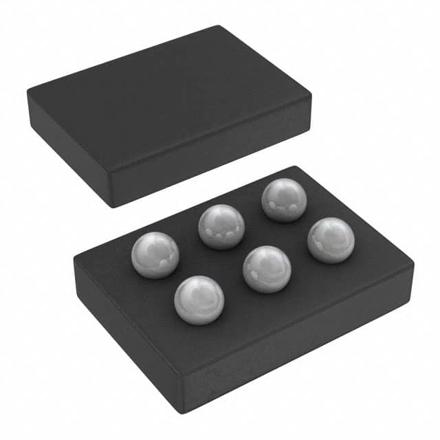
The MOSFET is housed in a 6-pin DSBGA wafer-level package measuring 1x1.5mm with a low profile of 0.62mm height, making it suitable for space-constrained applications. It is rated for operation from -55°C to 150°C junction temperature and has a maximum power dissipation of 1.5W on a standard FR4 PCB with 1in2 copper. The device is RoHS, Halogen Free, and Pb Free compliant.
Typical applications include battery management, load switching, and battery protection circuits where small size and efficient power handling are required. The device is supplied in tape and reel packaging with 3000 units per reel.
| Qty | Low | High |
|---|---|---|
| 1+ | $0.18 | $0.18 |
Estimated market price range - modelled values for guidance only, not live distributor offers.
The maximum drain-to-source voltage (Vds) is 20V.
The continuous drain current is 2.2A at Tc = 25°C.
The typical on-resistance is 62 mOhm and maximum is 75 mOhm at Vgs = -4.5V and Id = -1A.
The operating junction temperature range is -55°C to 150°C.
It comes in a 6-pin DSBGA (1x1.5mm) wafer-level package.
Yes, it is RoHS3 compliant, Halogen Free, and Pb Free.
The total gate charge is 1.9 nC typical and 2.5 nC maximum at Vgs = 4.5V.