

| Distributor | Stock | Pricing | MOQ | PKG | Lead Time | Date Code | On Order Quantity | On Order Delivery | |
|---|---|---|---|---|---|---|---|---|---|
|
32,873 pcs
|
32873 pcs | On Request | 1 | On Request | On Request | On Request | On Request | On Request | |
|
18,084 pcs
|
18084 pcs | On Request | 1 | On Request | On Request | 20+ | On Request | On Request | |
|
5,412 pcs
|
5412 pcs | On Request | 1 | On Request | On Request | 21+ | On Request | On Request | |
|
1,611 pcs
|
1611 pcs | On Request | 1 | On Request | On Request | On Request | On Request | On Request | |
|
1,420 pcs
|
1420 pcs | On Request | 1 | On Request | On Request | On Request | On Request | On Request | |
|
77 pcs
|
77 pcs | On Request | 1 | On Request | On Request | On Request | On Request | On Request | |
|
4 pcs
|
4 pcs | On Request | 1 | On Request | On Request | 21+ | On Request | On Request |
| Category | |
| Manufacturer Name | |
| Current | |
| Drain to Source Voltage (Vdss) | |
| Drive Voltage (Max Rds On, Min Rds On) | |
| FET Type | |
| Gate Charge (Qg) (Max) @ Vgs | |
| Halogen Free | |
| Input Capacitance (Ciss) (Max) @ Vds | |
| Mounting Type | |
| Operating Temperature | |
| Package / Case | |
| Power Dissipation (Max) | |
| Rds On (Max) @ Id, Vgs | |
| Supplier Device Package | |
| Tape & Reel | |
| Technology | |
| Vgs (Max) | |
| Vgs(th) (Max) @ Id |
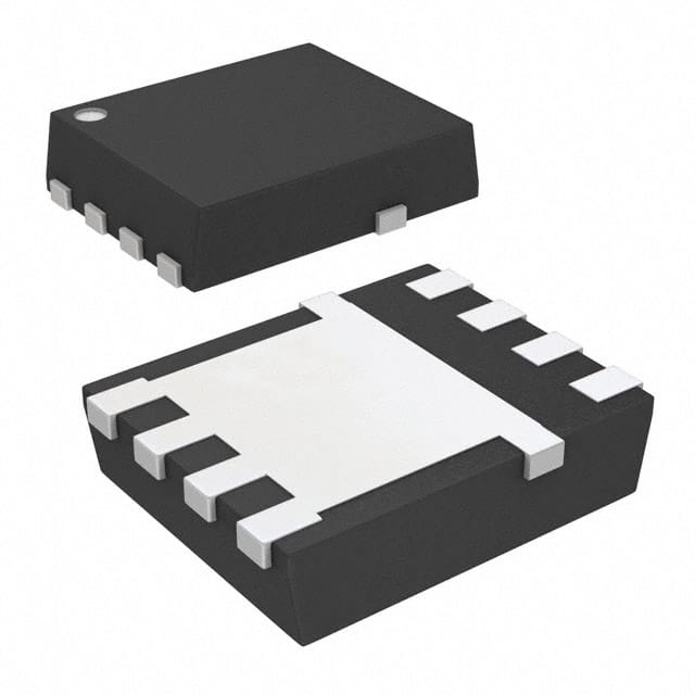
The CSD18540Q5B is a 60V N-Channel NexFET power MOSFET designed to minimize losses in power conversion applications. It features a typical on-resistance of 1.8mΩ at 10V and a maximum of 2.2mΩ, enabling high efficiency in DC-DC converters, secondary side synchronous rectifiers, isolated converter primary side switches, and motor control circuits. The device is logic level compatible, with a typical threshold voltage of 1.9V, and offers low gate charge (41 nC typical) and low thermal resistance. It is avalanche rated and supports continuous drain current up to 100A (package limited) or 205A (silicon limited at Tc=25°C). The MOSFET is housed in a SON 5mm x 6mm plastic package with lead-free terminal plating and is RoHS and halogen free compliant.
| Qty | Low | High |
|---|---|---|
| 1+ | $3.17 | $3.17 |
| 10+ | $1.89 | $1.89 |
| 100+ | $1.41 | $1.41 |
| 500+ | $1.19 | $1.19 |
| 1,000+ | $1.13 | $1.13 |
| 2,500+ | $1.08 | $1.08 |
Estimated market price range - modelled values for guidance only, not live distributor offers.
The maximum drain-to-source voltage is 60 V.
The package-limited continuous drain current is 100 A at TA=25°C. The silicon-limited current is 205 A at TC=25°C.
The typical on-resistance is 1.8 mΩ at VGS=10V, with a maximum of 2.2 mΩ at ID=28A.
The operating temperature range is -55°C to 175°C (junction and storage).
Yes, the device is RoHS compliant (RoHS3) and also halogen free with lead-free terminal plating.
The package is a SON 5mm x 6mm plastic package, also referred to as 8-PowerTDFN or 8-VSON-CLIP (5x6).
The typical total gate charge (Qg) is 41 nC at VGS=10V, with a maximum of 53 nC.