

| Distributor | Stock | Pricing | MOQ | PKG | Lead Time | Date Code | On Order Quantity | On Order Delivery | |
|---|---|---|---|---|---|---|---|---|---|
|
167 pcs
|
167 pcs | On Request | 1 | On Request | On Request | 17+ | On Request | On Request | |
|
115 pcs
|
115 pcs | On Request | 1 | On Request | On Request | 2026-02-25 06:16:38 | On Request | On Request |
| Category | |
| Manufacturer Name | |
| Current | |
| Drain to Source Voltage (Vdss) | |
| Drive Voltage (Max Rds On, Min Rds On) | |
| FET Type | |
| Gate Charge (Qg) (Max) @ Vgs | |
| Halogen Free | |
| Input Capacitance (Ciss) (Max) @ Vds | |
| Mounting Type | |
| Operating Temperature | |
| Power Dissipation (Max) | |
| Rds On (Max) @ Id, Vgs | |
| Storage Temperature | |
| Supplier Device Package | |
| Technology | |
| Vgs (Max) | |
| Vgs(th) (Max) @ Id |
The CSD16322Q5C is an N-Channel NexFET power MOSFET from Texas Instruments, designed for high-efficiency power conversion applications. It supports a maximum drain-to-source voltage of 25V and a gate-to-source voltage range of +10V to -8V. The device delivers continuous drain current of 21A at 25°C ambient temperature and 97A at 25°C case temperature, with a pulsed drain current rating of 136A.
On-state resistance is exceptionally low, with typical values of 3.9mOhm at VGS=8V, 4.6mOhm at VGS=4.5V, and 5.4mOhm at VGS=3V, all measured at ID=20A. The maximum RDS(on) is 5mOhm at VGS=8V. Gate charge is minimized at 6.8nC typical (9.7nC max) at VGS=4.5V, with gate-to-drain charge of 1.3nC, enabling fast switching and reduced driver losses. Input capacitance is 1365pF maximum at VDS=12.5V.
The device is avalanche rated with a single-pulse avalanche energy of 125mJ (ID=50A, L=0.1mH, RG=25Ω). It operates over a junction temperature range of -55°C to 150°C, with maximum power dissipation of 3.1W at 25°C ambient. The CSD16322Q5C is optimized for 5V gate drive applications and features the DualCool package for two-sided cooling.
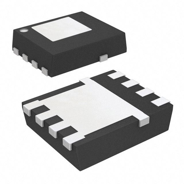
Packaged in an 8-PowerTDFN (SON 5x6mm) surface-mount package with supplier device package 8-SON, the CSD16322Q5C is RoHS3 compliant and halogen free. It is suitable for point-of-load synchronous buck converters in networking, telecom, and computing systems, and can be used as a synchronous or control FET.
The maximum drain-to-source voltage (VDS) is 25V.
The continuous drain current is 21A at TA=25°C and 97A at TC=25°C.
The typical on-state resistance is 3.9mOhm at VGS=8V, 4.6mOhm at VGS=4.5V, and 5.4mOhm at VGS=3V, all at ID=20A. The maximum is 5mOhm at VGS=8V.
The operating junction temperature range is -55°C to 150°C.
Yes, the CSD16322Q5C is RoHS3 compliant and halogen free.
The CSD16322Q5C is available in an 8-PowerTDFN package (SON 5x6mm) with supplier device package 8-SON, for surface-mount mounting.
The total gate charge is 6.8nC typical (9.7nC max) at VGS=4.5V, with gate-to-drain charge of 1.3nC typical.