

| Distributor | Stock | Pricing | MOQ | PKG | Lead Time | Date Code | On Order Quantity | On Order Delivery | |
|---|---|---|---|---|---|---|---|---|---|
|
17,480 pcs
|
17480 pcs | On Request | 1 | On Request | On Request | On Request | On Request | On Request | |
|
1,875 pcs
|
1875 pcs | On Request | 1 | On Request | On Request | 1249+ | On Request | On Request |
| Category | |
| Manufacturer Name | |
| AEC Qualified | |
| Automotive Grade | |
| Current | |
| Features | |
| Input Type | |
| Latch-up Performance | |
| Logic Type | |
| Mounting Type | |
| Number of Bits per Element | |
| Number of Channels | |
| Number of Elements | |
| Operating Temperature | |
| Operating Temperature Range | |
| Output Type | |
| Supplier Device Package | |
| Voltage |
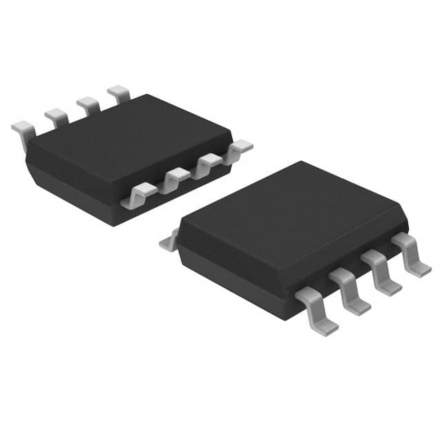
The Texas Instruments CLVC2G125IDCTRQ1 is a dual bus buffer gate designed for automotive applications, supporting a wide supply voltage range from 1.65V to 5.5V. This device features two line drivers with 3-state outputs, which are disabled when the output-enable (OE) input is high. It is fully specified for partial-power-down applications using Ioff circuitry, which prevents damaging current backflow when the device is powered down.
Key electrical characteristics include a maximum propagation delay of 4.3 ns at 3.3V and an output drive of ±24 mA at 3.3V. The buffer operates within an ambient temperature range of -40°C to 85°C. The device is available in SM8, 8-LSSOP, and 8-MSOP packages.
This buffer gate is suitable for various interface applications requiring signal buffering and level shifting within the specified voltage range. Its features, such as over-voltage tolerant inputs and very high speed, make it a versatile component for automotive designs.
| Qty | Low | High |
|---|---|---|
| 1+ | $0.33 | $0.33 |
Estimated market price range - modelled values for guidance only, not live distributor offers.
The device operates from 1.65V to 5.5V.
The operating temperature range is -40°C to 85°C.
The outputs are 3-state.
The maximum propagation delay is 4.3 ns at 3.3V.
The outputs can source up to 32 mA and sink up to 32 mA.
Yes, the device is automotive rated.
The device is available in 8-pin SSOP (DCT), 8-pin VSSOP (DCU), and SM8 packages.