

| Distributor | Stock | Pricing | MOQ | PKG | Lead Time | Date Code | On Order Quantity | On Order Delivery | |
|---|---|---|---|---|---|---|---|---|---|
|
95,389 pcs
|
95389 pcs | On Request | 1 | On Request | On Request | On Request | On Request | On Request | |
|
2,500 pcs
|
2500 pcs | On Request | 1 | On Request | On Request | On Request | On Request | On Request | |
|
8 pcs
|
8 pcs | On Request | 1 | On Request | On Request | On Request | On Request | On Request |
| Category | |
| Manufacturer Name | |
| Current | |
| ESD Protection | |
| Latch-up Performance | |
| Logic Type | |
| Mounting Type | |
| Number of Bits per Element | |
| Number of Elements | |
| Operating Temperature | |
| Output Type | |
| Propagation Delay | |
| Supplier Device Package | |
| Supplier Package | |
| Supply Current | |
| Voltage |
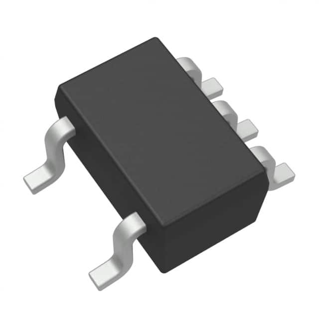
The Texas Instruments CLVC1G125MDCKREP is an enhanced product buffer featuring a single non-inverting element with 3-state outputs. This device is designed for operation across a wide voltage range, from 1.65V to 5.5V, making it suitable for various interfacing applications. It boasts a high-speed performance with a maximum propagation delay of 3.7 ns at 3.3V and offers a significant output drive capability of ±24mA at 3.3V.
The buffer operates within an extended temperature range of -55°C to 125°C, ensuring reliable performance in demanding environments. Key features include over-voltage tolerant inputs, partial power-down (Ioff) capability, and balanced outputs. The component is housed in a compact SC-70-5 package, suitable for surface mounting.
This buffer is qualified according to JEDEC and industry standards, including tests like Highly Accelerated Stress Test (HAST) and temperature cycling, to ensure reliable operation over its specified temperature range. It also meets stringent ESD protection levels, exceeding JESD 22 standards for the Human-Body Model, Machine Model, and Charged-Device Model.
| Qty | Low | High |
|---|---|---|
| 1+ | $0.93 | $0.93 |
Estimated market price range - modelled values for guidance only, not live distributor offers.
The operating voltage range is 1.65V to 5.5V.
It is available in the SC-70-5 package (also known as SOT-353).
The operating temperature range is -55°C to 125°C.
The output type is 3-State.
The output can source and sink 32mA each.
The typical propagation delay is 3.7ns at 3.3V.
Yes, it exceeds JESD 22 standards for ESD protection.