

| Distributor | Stock | Pricing | MOQ | PKG | Lead Time | Date Code | On Order Quantity | On Order Delivery | |
|---|---|---|---|---|---|---|---|---|---|
|
21,705 pcs
|
21705 pcs | On Request | 1 | On Request | On Request | On Request | On Request | On Request | |
|
7,000 pcs
|
7000 pcs | On Request | 1 | On Request | On Request | 0943+ | On Request | On Request | |
|
782 pcs
|
782 pcs | On Request | 1 | On Request | On Request | 02+ | On Request | On Request |
| Category | |
| Manufacturer Name | |
| AEC Qualified | |
| Automotive Grade | |
| Differential | |
| Divider | |
| Frequency | |
| Halogen Free | |
| Industrial Grade | |
| Input | |
| Input Type | |
| Mounting Type | |
| Number of Circuits | |
| Number of Outputs | |
| Operating Temperature | |
| Operating Temperature Range | |
| Output | |
| Output Type | |
| PLL | |
| Quiescent Current | |
| Ratio | |
| Supplier Device Package | |
| Supplier Package | |
| Supply Voltage | |
| Tape & Reel | |
| Type | |
| Voltage |
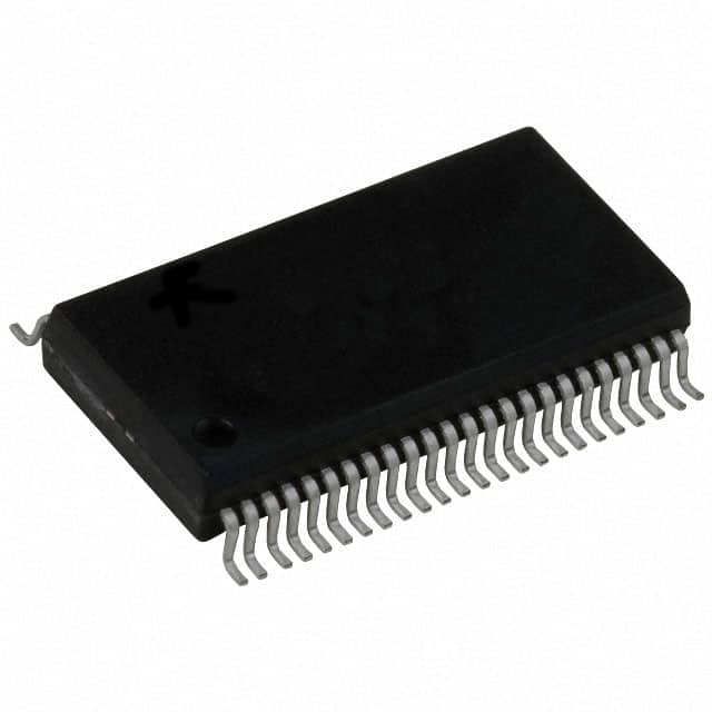
The CDCVF857DGGR from Texas Instruments is a high-performance, low-skew, low-jitter, zero-delay buffer designed for DDR memory modules. It distributes a differential clock input to 10 differential clock output pairs and one differential feedback clock output pair.
Key electrical specifications include a core supply voltage of 2.5V and an output supply voltage of 1.7V. The device offers an output skew of 75 ps and operates within a frequency range of 60 MHz to 220 MHz. It boasts low jitter characteristics, with cycle-cycle jitter of ±35 ps and period jitter of ±30 ps. The input and output types are LVTTL and SSTL-2 compatible.
This clock driver is available in a 48-TSSOP package and supports surface mount installation. It operates across a temperature range of -40°C to 85°C. The CDCVF857DGGR meets or exceeds JEDEC standards JESD82-1 for DDR I-200/266/333 and the proposed JESD82-1A for DDR I-400.
Applications include DDR memory modules (DDR400/333/266/200) and zero-delay fan-out buffer requirements. The device enters a low-power mode when no CLK input signal is applied or PWRDWN is low.
| Qty | Low | High |
|---|---|---|
| 1+ | $5.38 | $5.38 |
Estimated market price range - modelled values for guidance only, not live distributor offers.
The operating voltage range is 2.3V to 2.7V, with a core supply voltage of 2.5V and an output supply voltage of 1.7V.
The CDCVF857DGGR is available in a 48-TSSOP package.
The operating temperature range is -40°C to 85°C.
The RoHS status is RoHS3 Compliant.
The CDCVF857DGGR has 10 outputs.
The output skew is 75 ps.
The typical additive RMS jitter is 30 fs.