

| Distributor | Stock | Pricing | MOQ | PKG | Lead Time | Date Code | On Order Quantity | On Order Delivery | |
|---|---|---|---|---|---|---|---|---|---|
|
15,067 pcs
|
15067 pcs | On Request | 1 | On Request | On Request | On Request | On Request | On Request | |
|
8,674 pcs
|
8674 pcs | On Request | 1 | On Request | On Request | On Request | On Request | On Request |
| Category | |
| Manufacturer Name | |
| Conflict Minerals | |
| Differential | |
| Divider | |
| Frequency | |
| Halogen Free | |
| Input | |
| Input Type | |
| Lead Spacing | |
| Lead Style | |
| Mounting Type | |
| Number of Circuits | |
| Number of Outputs | |
| Operating Temperature | |
| Operating Temperature Range | |
| Output | |
| Output Type | |
| PLL | |
| Quiescent Current | |
| Ratio | |
| SVHC Present | |
| Supplier Device Package | |
| Supply Voltage | |
| Tape & Reel | |
| Type | |
| Voltage |
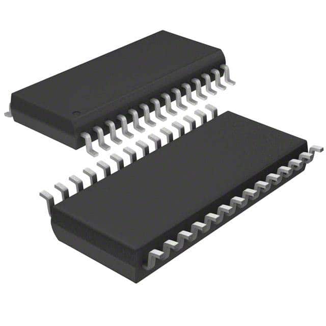
The CDCVF855PWR from Texas Instruments is a high-performance PLL Clock Driver. It is designed to distribute clock signals with low skew and jitter, making it suitable for demanding applications. This device features 4 outputs and supports a core supply voltage of 2.5V, with an output supply voltage of 1.7V.
The operating temperature range for the CDCVF855PWR is -40°C to 85°C, ensuring reliable performance in various environments. It comes in a 28-TSSOP package, suitable for surface mount applications. The device supports SSTL-2 input and output types and operates at frequencies up to 220MHz.
Key specifications include low additive RMS jitter of 65 fs (typical), output skew of 40 ps, and low static phase offset of ±50 ps. It meets or exceeds JEDEC standards for DDR memory modules, including DDR1-200/266/333 and proposed DDR1-400 specifications. The device also includes a low-power mode that activates when no CLK input signal is applied or PWRDWN is low.
| Qty | Low | High |
|---|---|---|
| 1+ | $2.12 | $2.12 |
Estimated market price range - modelled values for guidance only, not live distributor offers.
The operating temperature range is -40°C to 85°C.
The CDCVF855PWR is available in a 28-TSSOP package.
The core supply voltage is 2.5V.
The CDCVF855PWR has 4 outputs.
The maximum operating frequency is 220 MHz.
The typical additive RMS jitter is 65 fs.
Yes, it meets/exceeds JEDEC Standard JESD82-1 for DDR1-200/266/333 and proposed DDR1-400 Specification JESD82-1A.