

| Distributor | Stock | Pricing | MOQ | PKG | Lead Time | Date Code | On Order Quantity | On Order Delivery | |
|---|---|---|---|---|---|---|---|---|---|
|
11,682 pcs
|
11682 pcs | On Request | 1 | On Request | On Request | On Request | On Request | On Request | |
|
4,364 pcs
|
4364 pcs | On Request | 1 | On Request | On Request | 24+ | On Request | On Request | |
|
2,220 pcs
|
2220 pcs | On Request | 1 | On Request | On Request | On Request | On Request | On Request | |
|
466 pcs
|
466 pcs | On Request | 1 | On Request | On Request | 10+ | On Request | On Request |
| Category | |
| Manufacturer Name | |
| Differential | |
| Divider | |
| Frequency | |
| Input | |
| Lead Spacing | |
| Mounting Type | |
| Number of Circuits | |
| Operating Temperature | |
| Output | |
| PLL | |
| Ratio | |
| Supplier Device Package | |
| Supplier Package | |
| Tape & Reel | |
| Type | |
| Voltage |
The CDCVF2510PWR from Texas Instruments is a high-performance, low-skew, low-jitter, phase-lock loop (PLL) clock driver. It is designed to meet and exceed PC133 SDRAM Registered DIMM Specification Rev. 1.1 and is compatible with spread spectrum clocking.
This device operates at 3.3V and supports frequencies from 50 MHz to 175 MHz. It features a 2:11 ratio, distributing one clock input to one bank of 10 outputs. The outputs are synchronized to the clock input via an external feedback (FBIN) terminal. Integrated 25-ohm on-chip series damping resistors eliminate the need for an external RC network.
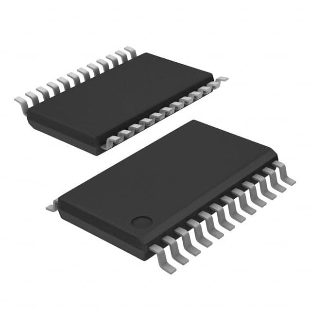
The CDCVF2510PWR operates within a temperature range of 0°C to 85°C. It is available in a 24-pin TSSOP package, suitable for surface mounting. The device is ideal for driving point-to-point loads in synchronous DRAM applications, providing low-skew, low-jitter copies of the clock signal with a 50% duty cycle independent of the input clock duty cycle.
The CDCVF2510PWR operates at 3.3V.
The CDCVF2510PWR is available in a 24-TSSOP package.
The operating temperature range for the CDCVF2510PWR is 0°C to 85°C.
The maximum operating frequency for the CDCVF2510PWR is 175 MHz.
The static phase error distribution at 66 MHz to 166 MHz is ±125 ps.
The cycle-to-cycle jitter at 66 MHz to 166 MHz is |70| ps.