

| Distributor | Stock | Pricing | MOQ | PKG | Lead Time | Date Code | On Order Quantity | On Order Delivery | |
|---|---|---|---|---|---|---|---|---|---|
|
13,220 pcs
|
13220 pcs | On Request | 1 | On Request | On Request | On Request | On Request | On Request | |
|
3,164 pcs
|
3164 pcs | On Request | 1 | On Request | On Request | 09+ | On Request | On Request |
| Category | |
| Manufacturer Name | |
| Differential | |
| Divider | |
| Frequency | |
| Input | |
| Input Type | |
| Mounting Type | |
| Number of Circuits | |
| Number of Outputs | |
| Operating Temperature | |
| Operating Temperature Range | |
| Output | |
| Output Type | |
| PLL | |
| Ratio | |
| Supplier Device Package | |
| Type | |
| Voltage |
The CDCVF2510APWR is an integrated circuit manufactured by Texas Instruments, categorized under clock generators, PLLs, and frequency synthesizers. It functions as a PLL clock driver with ten outputs, suitable for applications requiring multiple synchronized clock signals. The device operates at a core supply voltage of 3.3V and has an output supply voltage of 3.3V, making it compatible with standard digital logic levels.
This clock driver features an additive RMS jitter of 70 femtoseconds and an output skew of 100 picoseconds, ensuring precise timing performance. Its static phase error distribution is ±125 picoseconds, and jitter (cyc–cyc) is approximately 70 picoseconds. The operating temperature range spans from 0°C to 85°C, suitable for various industrial and consumer applications. The device uses LVTTL input and output types, supporting a wide frequency range from 20 MHz to 175 MHz.
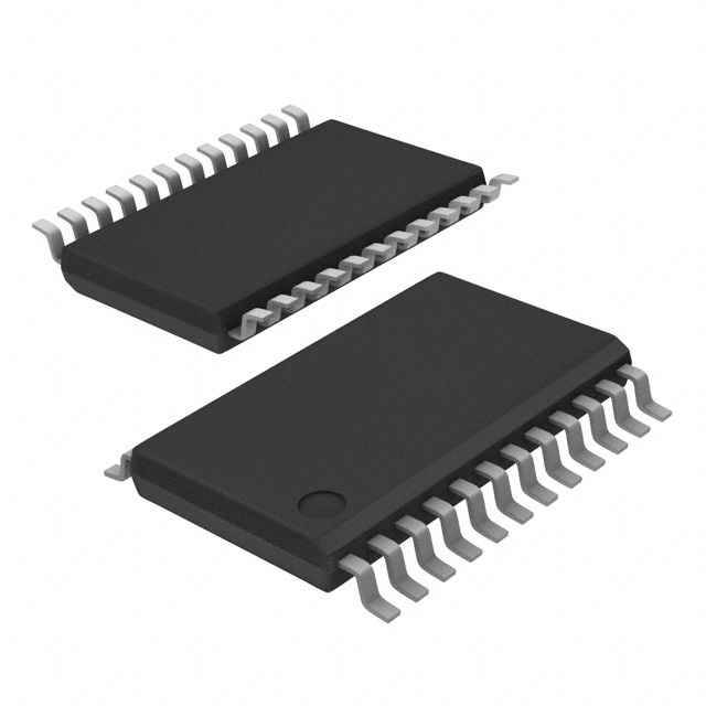
The CDCVF2510APWR is packaged in a 24-TSSOP package, facilitating surface-mount assembly. It is designed for use in systems requiring multiple clock signals with high timing accuracy, such as communication equipment, data processing systems, and instrumentation.
| Qty | Low | High |
|---|---|---|
| 1+ | $2.77 | $2.77 |
Estimated market price range - modelled values for guidance only, not live distributor offers.
The device operates at a voltage of 3.3V, supporting a voltage range of 3V to 3.6V.
The operating temperature range is from 0°C to 85°C.