

| Distributor | Stock | Pricing | MOQ | PKG | Lead Time | Date Code | On Order Quantity | On Order Delivery | |
|---|---|---|---|---|---|---|---|---|---|
|
13,225 pcs
|
13225 pcs | On Request | 1 | On Request | On Request | On Request | On Request | On Request | |
|
8,083 pcs
|
8083 pcs | On Request | 1 | On Request | On Request | 05+ | On Request | On Request | |
|
120 pcs
|
120 pcs | On Request | 1 | On Request | On Request | 1244+ | On Request | On Request |
| Category | |
| Manufacturer Name | |
| Differential | |
| Divider | |
| Frequency | |
| Input | |
| Input Type | |
| Mounting Type | |
| Number of Circuits | |
| Number of Outputs | |
| Operating Temperature | |
| Output | |
| PLL | |
| Ratio | |
| Supplier Device Package | |
| Supplier Package | |
| Type | |
| Voltage |
The CDCVF2509PW from Texas Instruments is a high-performance, low-skew, low-jitter phase-lock loop (PLL) clock driver designed for synchronous DRAM applications. It operates at a 3.3V core and output supply voltage, distributing one clock input to nine outputs. The device features one bank of five outputs and another bank of four outputs, each with a separate output enable.
Key electrical specifications include an operating frequency range of 50MHz to 175MHz, an additive RMS jitter of 70fs (typical), and an output skew of 100ps. The static phase error distribution is ±125ps at 66MHz to 166MHz. The CDCVF2509PW includes on-chip series damping resistors, eliminating the need for external RC networks and driving point-to-point loads effectively.
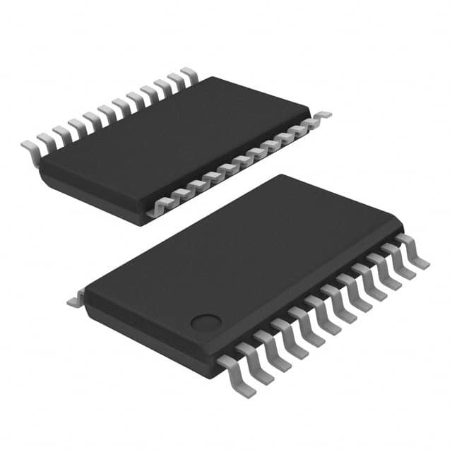
This clock driver is available in a 24-pin TSSOP package, suitable for surface mounting. It is designed to meet and exceed the PC133 SDRAM registered DIMM specification Rev. 1.1 and is spread spectrum clock-compatible. The advanced deep submicron process contributes to lower power consumption compared to previous generations.
Applications include clock distribution for synchronous DRAM, memory modules, and other high-speed digital systems requiring precise clock synchronization and low jitter.
| Qty | Low | High |
|---|---|---|
| 1+ | $7.30 | $7.30 |
Estimated market price range - modelled values for guidance only, not live distributor offers.
The core supply voltage is 3.3V.
The CDCVF2509PW has 9 outputs.
The output type is LVTTL.
The operating temperature range is 0°C to 85°C.
The maximum operating frequency is 175MHz.
The typical additive RMS jitter is 70fs.
The CDCVF2509PW is supplied in a 24-TSSOP package.