

| Distributor | Stock | Pricing | MOQ | PKG | Lead Time | Date Code | On Order Quantity | On Order Delivery | |
|---|---|---|---|---|---|---|---|---|---|
|
2,010 pcs
|
2010 pcs | On Request | 1 | On Request | On Request | 24+ | On Request | On Request | |
|
18 pcs
|
18 pcs | On Request | 1 | On Request | On Request | On Request | On Request | On Request |
| Category | |
| Manufacturer Name | |
| Contact Plating | |
| Differential | |
| Divider | |
| Frequency | |
| Height | |
| Input | |
| Input Type | |
| Length | |
| Mounting Type | |
| Number of Circuits | |
| Number of Outputs | |
| Operating Temperature | |
| Output | |
| PLL | |
| Package Quantity | |
| Power Dissipation | |
| Ratio | |
| Supplier Device Package | |
| Type | |
| Voltage | |
| Width |
The Texas Instruments CDCVF2509APW is a 3.3-Volt Phase-Lock Loop (PLL) clock driver designed for clock distribution applications. It features a single circuit with 9 LVTTL outputs, capable of handling frequencies up to 175MHz.
This clock buffer/driver operates within a supply voltage range of 3V to 3.6V and has a low operating supply current of 40µA. The device is specified for an operating temperature range of 0°C to 85°C and has a power dissipation of 700mW.
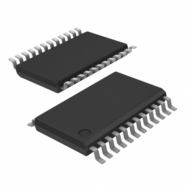
Packaged in a 24-TSSOP with gold contact plating, the CDCVF2509APW measures 7.8mm x 4.4mm x 1.15mm. It is designed for surface mounting and comes in a rail/tube package quantity of 60 units. The component is RoHS compliant and lead-free.
The CDCVF2509APW operates at 3.3V supply voltage.
The maximum frequency supported is 175MHz.
It has 9 outputs.
It is housed in a 24-TSSOP package.
The operating temperature range is 0°C to 85°C.
RoHS compliance status is unverified.
The power dissipation is 700mW.