

| Distributor | Stock | Pricing | MOQ | PKG | Lead Time | Date Code | On Order Quantity | On Order Delivery | |
|---|---|---|---|---|---|---|---|---|---|
|
6,027 pcs
|
6027 pcs | On Request | 1 | On Request | On Request | On Request | On Request | On Request | |
|
4,373 pcs
|
4373 pcs | On Request | 1 | On Request | On Request | On Request | On Request | On Request |
| Category | |
| Manufacturer Name | |
| Differential | |
| Divider | |
| Frequency | |
| Input | |
| Mounting Type | |
| Number of Circuits | |
| Operating Temperature | |
| Output | |
| PLL | |
| Ratio | |
| Supplier Device Package | |
| Supplier Package | |
| Type | |
| Voltage |
The CDCVF25084PW is an integrated circuit from Texas Instruments that functions as a clock multiplier. It provides a frequency multiplication ratio of 2:8, specifically 1:8 X4, suitable for timing and frequency synthesis in electronic systems. The device operates at a supply voltage of 3.3V and supports input frequencies from 2.5 MHz to 45 MHz, with output frequencies ranging from 10 MHz to 180 MHz. It features LVTTL input and output types, making it compatible with standard digital logic levels.
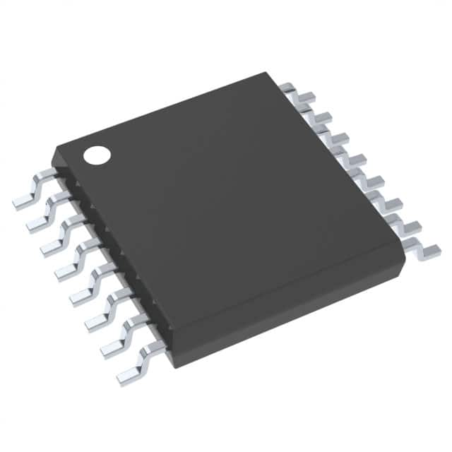
Designed for surface mounting, the device comes in a 16-TSSOP package with a width of 0.173 inches (4.40 mm). It includes PLL functionality with bypass options and has an additive RMS jitter of 120 femtoseconds, with an output skew of 150 picoseconds. The IC is suitable for applications requiring precise clock generation and frequency synthesis, such as communication systems, test equipment, and digital signal processing.
Environmental compliance data indicates RoHS3 compliance, with a Moisture Sensitivity Level of 1, and REACH unaffected status. The device's design considerations include low jitter and stable output skew, making it appropriate for high-performance timing applications.
| Qty | Low | High |
|---|---|---|
| 1+ | $6.76 | $6.76 |
Estimated market price range - modelled values for guidance only, not live distributor offers.
The CDCVF25084PW operates at 3.3V.
It comes in a 16-TSSOP package.
-40°C to 85°C.
Yes, it is RoHS3 compliant.