

| Distributor | Stock | Pricing | MOQ | PKG | Lead Time | Date Code | On Order Quantity | On Order Delivery | |
|---|---|---|---|---|---|---|---|---|---|
|
42,152 pcs
|
42152 pcs | On Request | 1 | On Request | On Request | On Request | On Request | On Request | |
|
12,053 pcs
|
12053 pcs | On Request | 1 | On Request | On Request | On Request | On Request | On Request | |
|
2,125 pcs
|
2125 pcs | On Request | 1 | On Request | On Request | 10+ | On Request | On Request | |
|
967 pcs
|
967 pcs | On Request | 1 | On Request | On Request | On Request | On Request | On Request |
| Category | |
| Manufacturer Name | |
| Differential | |
| Divider | |
| Frequency | |
| Input | |
| Input Type | |
| Mounting Type | |
| Number of Circuits | |
| Number of Outputs | |
| Operating Temperature | |
| Output | |
| Output Type | |
| PLL | |
| Ratio | |
| Supplier Device Package | |
| Supplier Package | |
| Type | |
| Voltage |
The CDCVF25081PWR from Texas Instruments is a high-performance, low-skew, low-jitter phase-locked loop (PLL) clock driver. This device utilizes a PLL to precisely align output clocks in both frequency and phase with the input clock signal. It features 1 clock input to 2 banks of 4 outputs, totaling 8 buffered CLKIN outputs.
The CDCVF25081PWR operates with a supply voltage range of 3V to 3.6V and supports an operating frequency from 8 MHz to 200 MHz. Key electrical characteristics include an additive RMS jitter of 100 fs (typical) for 66 MHz to 200 MHz operation and an output skew of 150 ps. The device includes 25 Ω on-chip series damping resistors.
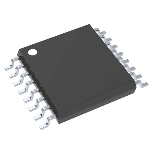
Designed for industrial applications, it operates within an ambient temperature range of -40°C to 85°C. The CDCVF25081PWR supports a power-down mode, consuming less than 20 µA. It is packaged in a 16-TSSOP (0.173", 4.40mm Width) surface-mount package.
| Qty | Low | High |
|---|---|---|
| 1+ | $1.94 | $1.94 |
Estimated market price range - modelled values for guidance only, not live distributor offers.
The CDCVF25081PWR operates with a supply voltage range of 3 V to 3.6 V.
The CDCVF25081PWR is available in a 16-TSSOP package.
The operating temperature range for the CDCVF25081PWR is -40°C to 85°C.
The CDCVF25081PWR is RoHS3 Compliant.
The CDCVF25081PWR has 8 outputs.
The typical additive RMS jitter for the CDCVF25081PWR is 100 fs for 66 MHz to 200 MHz operation.
The output skew of the CDCVF25081PWR is 150 ps.