

| Distributor | Stock | Pricing | MOQ | PKG | Lead Time | Date Code | On Order Quantity | On Order Delivery | |
|---|---|---|---|---|---|---|---|---|---|
|
22,600 pcs
|
22600 pcs | On Request | 1 | On Request | On Request | On Request | On Request | On Request | |
|
2,020 pcs
|
2020 pcs | On Request | 1 | On Request | On Request | 24+ | On Request | On Request | |
|
100 pcs
|
100 pcs | On Request | 1 | On Request | On Request | On Request | On Request | On Request |
| Category | |
| Manufacturer Name | |
| Differential | |
| Divider | |
| Frequency | |
| Input | |
| Input Type | |
| Mounting Type | |
| Number of Circuits | |
| Number of Outputs | |
| Operating Temperature | |
| Output | |
| Output Type | |
| PLL | |
| Ratio | |
| Supplier Device Package | |
| Supplier Package | |
| Type | |
| Voltage |
The CDCVF25081PW from Texas Instruments is a high-performance, low-skew, low-jitter phased-locked loop (PLL) clock driver. It is designed to precisely align output clocks in both frequency and phase to the input clock signal. This device features one clock input and provides 8 buffered CLKIN outputs, divided into two banks of four.
Key electrical specifications include a core and output supply voltage of 3.3V, with a range of 3V to 3.6V. It operates at frequencies from 8 MHz to 200 MHz. The additive RMS jitter is typically 100 fs, and output skew is 150 ps. The output type is LVTTL, and the input type is also LVTTL. The device includes 25-ohm on-chip series damping resistors.
For power efficiency, a power-down mode is available, consuming less than 20 µA. The operating temperature range is industrial, from -40°C to 85°C. The CDCVF25081PW supports Spread Spectrum Clocking (SSC) and features a fail-safe function. Input hysteresis prevents random output oscillation when no input signal is present.
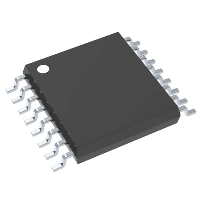
This clock driver is available in a 16-TSSOP package, suitable for surface mounting. The package dimensions are 5.0 mm x 4.4 mm. The device is designed for applications requiring precise clock distribution and synchronization.
| Qty | Low | High |
|---|---|---|
| 1+ | $2.32 | $2.32 |
Estimated market price range - modelled values for guidance only, not live distributor offers.
The CDCVF25081PW operates with a core and output supply voltage of 3.3V, and supports a range from 3V to 3.6V.
The CDCVF25081PW is available in a 16-TSSOP package, measuring 5.0 mm x 4.4 mm, and is designed for surface mounting.
The CDCVF25081PW is characterized for an operating temperature range of -40°C to 85°C.
The CDCVF25081PW is RoHS3 Compliant.
The CDCVF25081PW provides 8 LVTTL outputs.
The typical additive RMS jitter is 100 fs, and the cycle-cycle jitter is ±100 ps for frequencies between 66 MHz and 200 MHz.
The CDCVF25081PW can operate at frequencies up to 200 MHz.