

| Distributor | Stock | Pricing | MOQ | PKG | Lead Time | Date Code | On Order Quantity | On Order Delivery | |
|---|---|---|---|---|---|---|---|---|---|
|
17,858 pcs
|
17858 pcs | On Request | 1 | On Request | On Request | On Request | On Request | On Request | |
|
20 pcs
|
20 pcs | On Request | 1 | On Request | On Request | On Request | On Request | On Request |
| Category | |
| Manufacturer Name | |
| Differential | |
| Frequency | |
| Input | |
| Input Type | |
| Mounting Type | |
| Number of Circuits | |
| Number of Outputs | |
| Operating Temperature | |
| Operating Temperature Range | |
| Output | |
| Ratio | |
| Supplier Device Package | |
| Supplier Package | |
| Type | |
| Voltage |
The CDCVF2310MPWREP from Texas Instruments is a high-performance, low-skew clock buffer capable of distributing one clock input to ten outputs. It operates across a wide voltage range of 2.3V to 3.6V and supports core supply voltages of 2.5V and 3.3V. This device can function at frequencies up to 200 MHz at a 3.3V VDD.
Designed for general-purpose applications, the CDCVF2310MPWREP features LVTTL input and output types. It offers a pin-to-pin skew of less than 100 ps at 3.3V. The operating temperature range is specified from -40°C to 105°C, with support for 105°C ambient temperature. The buffer distributes the clock input into two banks of five outputs each, providing synchronized clock signals.
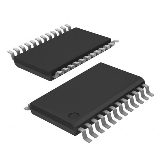
This clock buffer is packaged in a 24-pin TSSOP (Thin Shrink Small Outline Package). The device includes output enable glitch suppression for synchronized output enable sequences. Its design supports a 1:10 fanout ratio, making it suitable for various clock distribution needs in electronic systems.
| Qty | Low | High |
|---|---|---|
| 1+ | $15.31 | $15.31 |
Estimated market price range - modelled values for guidance only, not live distributor offers.
The CDCVF2310MPWREP operates with core supply voltages of 2.5V and 3.3V, and the overall voltage range is 2.3V to 3.6V.
This clock buffer operates up to 200 MHz at a VDD of 3.3V.
The operating temperature range is -40°C to 105°C.
The CDCVF2310MPWREP is supplied in a 24-TSSOP package.
The output skew is less than 100 ps at a VDD of 3.3V.